AGL250V2-QN144Y Ver la hoja de datos (PDF) - Microsemi Corporation
Número de pieza
componentes Descripción
Fabricante
AGL250V2-QN144Y Datasheet PDF : 250 Pages
| |||
IGLOO DC and Switching Characteristics
PLL Behavior at Brownout Condition
Microsemi recommends using monotonic power supplies or voltage regulators to ensure proper power-
up behavior. Power ramp-up should be monotonic at least until VCC and VCCPLX exceed brownout
activation levels (see Figure 2-1 and Figure 2-2 on page 2-5 for more details).
When PLL power supply voltage and/or VCC levels drop below the VCC brownout levels (0.75 V ± 0.25
V for V5 devices, and 0.75 V ± 0.2 V for V2 devices), the PLL output lock signal goes low and/or the
output clock is lost. Refer to the Brownout Voltage section in the "Power-Up/-Down Behavior of Low
Power Flash Devices" chapter of the ProASIC®3 and ProASIC3E FPGA fabric user’s guides for
information on clock and lock recovery.
Internal Power-Up Activation Sequence
1. Core
2. Input buffers
3. Output buffers, after 200 ns delay from input buffer activation
To make sure the transition from input buffers to output buffers is clean, ensure that there is no path
longer than 100 ns from input buffer to output buffer in your design.
VCC
VCC = 1.575 V
VCC = 1.425 V
Activation trip point:
Va = 0.85 V ± 0.25 V
Deactivation trip point:
Vd = 0.75 V ± 0.25 V
VCC = VCCI + VT
where VT can be from 0.58 V to 0.9 V (typically 0.75 V)
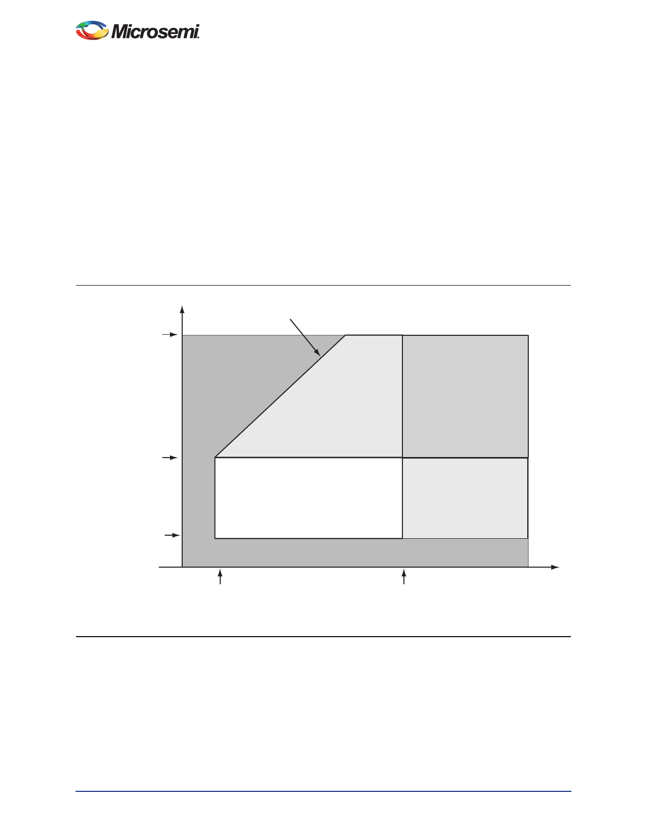
Region 1: I/O Buffers are OFF
Region 4: I/O
buffers are ON.
I/Os are functional
(except differential inputs)
but slower because VCCI
is below specification. For the
same reason, input buffers do not
meet VIH / VIL levels, and output
buffers do not meet VOH / VOL levels.
Region 2: I/O buffers are ON.
I/Os are functional (except differential inputs)
but slower because VCCI / VCC are below
specification. For the same reason, input
buffers do not meet VIH / VIL levels, and
output buffers do not meet VOH / VOL levels.
Region 1: I/O buffers are OFF
Region 5: I/O buffers are ON
and power supplies are within
specification.
I/Os meet the entire datasheet
and timer specifications for
speed, VIH / VIL, VOH / VOL,
etc.
Region 3: I/O buffers are ON.
I/Os are functional; I/O DC
specifications are met,
but I/Os are slower because
the VCC is below specification.
Activation trip point:
Va = 0.9 V ± 0.3 V
Deactivation trip point:
Vd = 0.8 V ± 0.3 V
Min VCCI datasheet specification
voltage at a selected I/O
standard; i.e., 1.425 V or 1.7 V
or 2.3 V or 3.0 V
Figure 2-1 • V5 Devices – I/O State as a Function of VCCI and VCC Voltage Levels
VCCI
2-4
Revision 23
Share Link: 