FS6012-02 Ver la hoja de datos (PDF) - AMI Semiconductor
Número de pieza
componentes Descripción
Fabricante
FS6012-02 Datasheet PDF : 20 Pages
| |||
X T
)6
,& 'LJLWDO 9LGHR$XGLR &ORFN *HQHUDWRU ,&
August 1998
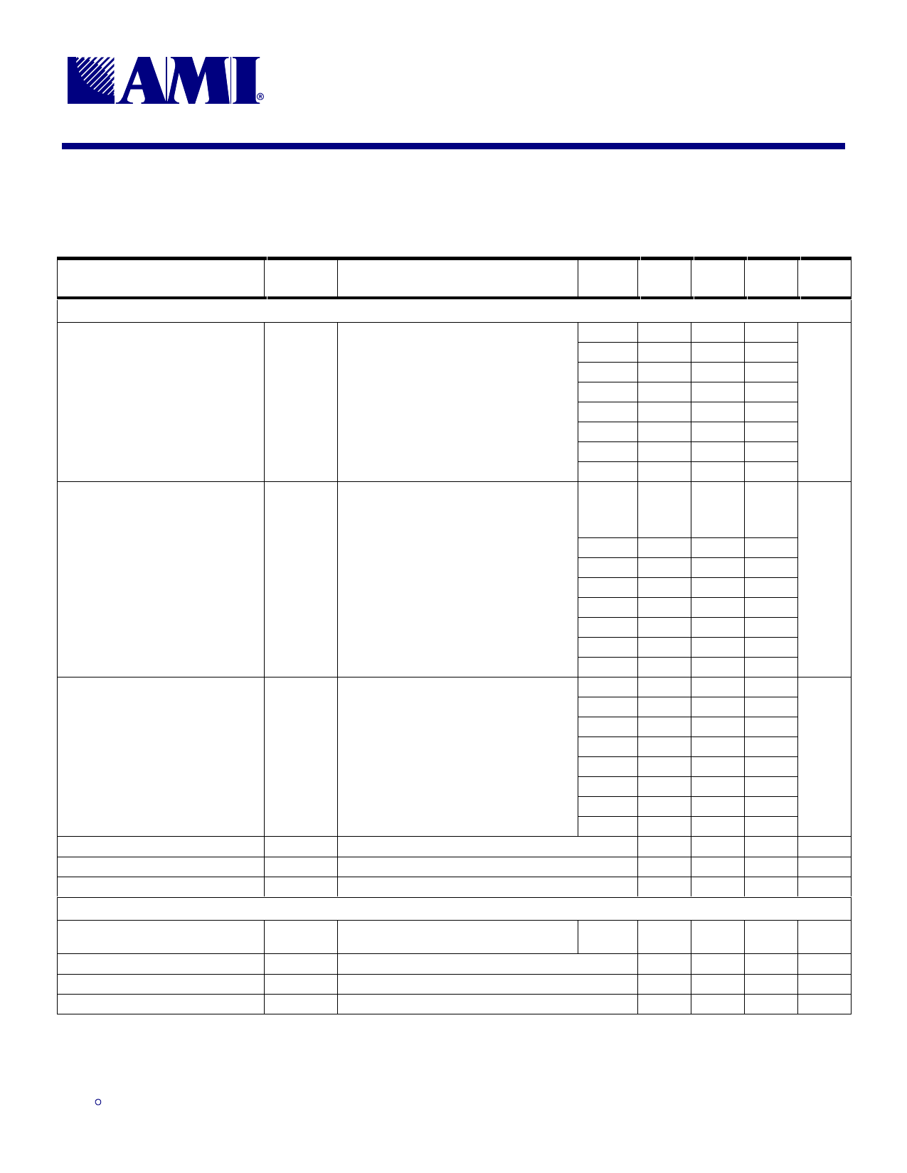
Table 11: AC Timing Specifications
Unless otherwise stated, VDD = 5.0V ± 10%, no load on any output, and ambient temperature range TA = 0°C to 70°C. Parameters denoted with an asterisk ( * ) represent nominal characterization
data and are not currently production tested to any specific limits. MIN and MAX characterization data are ± 3σ from typical.
PARAMETER
SYMBOL
CONDITIONS/DESCRIPTION
CLOCK
(MHz)
MIN.
TYP.
MAX. UNITS
Clock Output (PCLK)
Duty Cycle *
Jitter, Long Term (σy2(τ)) *
Jitter, Period (peak-peak) *
Clock Stabilization *
Rise Time *
Fall Time *
Clock Output (CLK27)
Duty Cycle *
Clock Stabilization Time *
Rise Time *
Fall Time *
14.318
48
52
17.734
48
52
3.579
48
52
From rising edge to rising edge at 2.5V
52.416
40
4.4342
48
44
%
52
4.4336
48
52
4.4335
48
52
19.440
48
14
.3
18
52
8
0
0
17.734
1410
tj(LT)
From rising edge to 1st rising edge after
500µs at 2.5V, CL = 15pF, all PLLs active
3.579
52.416
870
980
ps
4.4342
1070
4.4336
1300
4.4335
1630
19.440
1430
14.318
510
17.734
500
3.579
520
tj(∆P)
From rising edge to the next rising edge at
2.5V, CL = 15pF, all PLLs active
52.416
4.4342
620
680
ps
4.4336
750
4.4335
740
19.440
580
tSTB
Output active from power-up
960
µs
tr
VO = 0.5V to 4.5V; CL = 15pF
3.5
ns
tf
VO = 4.5V to 0.5V; CL = 15pF
1.8
ns
Crystal oscillator frequency out, from rising
edge to rising edge at 2.5V
27
tSTB
Output active from power-up
tr
VO = 0.5V to 4.5V; CL = 15pF
tf
VO = 4.5V to 0.5V; CL = 15pF
45
48
%
300
µs
3.5
ns
2.2
ns
,62
11
8.19.98
Share Link: 