VRS1000 Ver la hoja de datos (PDF) - Unspecified
Número de pieza
componentes Descripción
Fabricante
VRS1000 Datasheet PDF : 47 Pages
| |||
VRS1000
VERSA
Datasheet Rev 1.6
The transistor would be off (open-circuited) and current
would flow from the VCC to the pin, generating a
logical high at the output. Also, note that if an external
device with a logical low value is connected to the pin,
the current will flow out of the pin. In order to have a
real bi-directional output, the input should be in a high
impedance state. It is for this reason that we call ports
P1, P2, P3 and P4 “quasi bi-directional”.
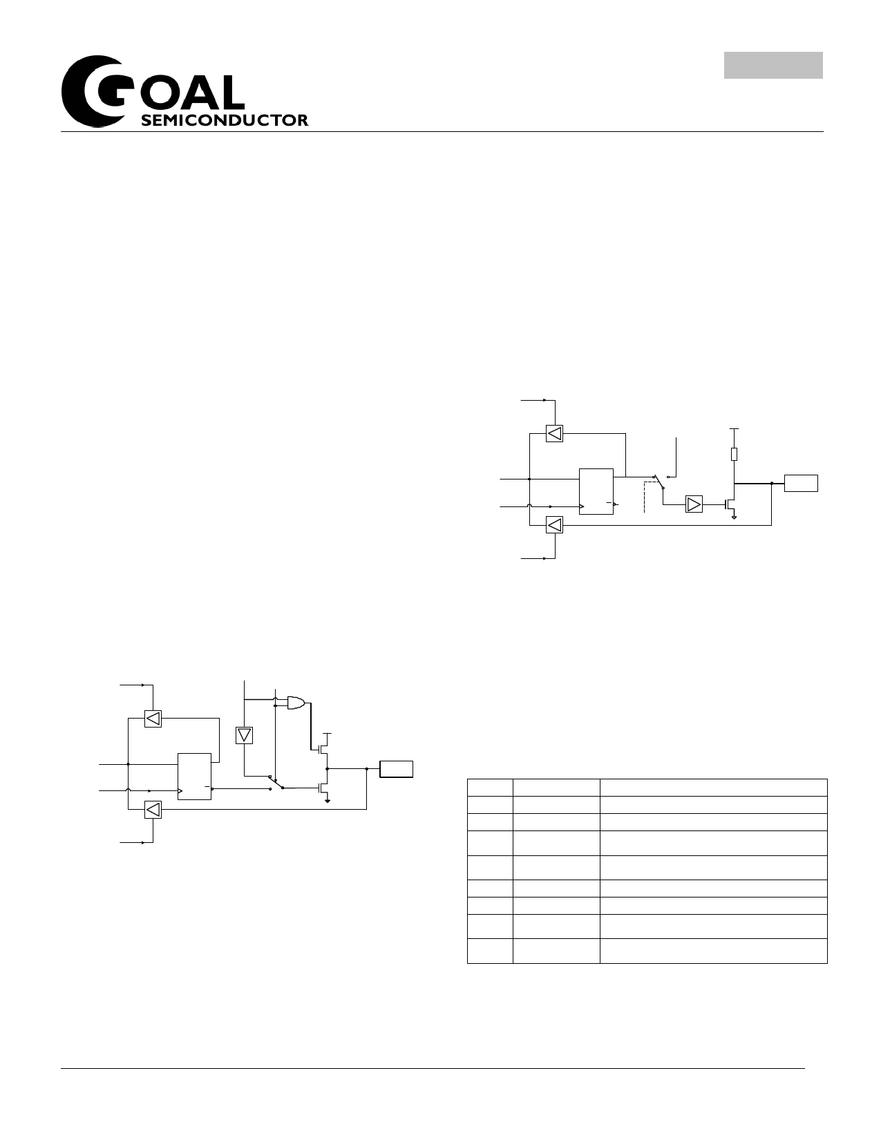
Structure of Port 0
The internal structure of P0 is shown in the next figure.
The auxiliary function of this port requires a particular
logic. As opposed to the other ports, P0 is truly bi-
directional. In other words, when used as an input, it is
considered to be in a floating logical state (high
impedance state). This arises from the absence of the
internal pull-up resistance. The pull-up resistance is
actually replaced by a transistor that is only used when
the port functions to access external memory/data bus
(EA=0).
When used as an I/O port, P0 acts as an open drain
port and the use of an external pull-up resistor is likely
to be required for most applications.
FIGURE 9: PORT P0’S PARTICULAR STRUCTURE
Read Register
Address A0/A7
Co ntr ol
Internal Bus
W rite t o
Register
Q
D Flip-Flop
Q
Vcc
X1
IC Pin
Read Pin
When P0 is used as an external memory bus input (for
a MOVX instruction, for example), the outputs of the
register are automatically forced to 1.
Port P0 and P2 as Address and Data Bus
The output stage may receive data from two sources
o The outputs of register P0 or the bus address
itself multiplexed with the data bus for P0.
o The outputs of the P2 register or the high part
(A8/A15) of the bus address for the P2 port.
FIGURE 10: P2 PORT STRUCTURE
Read Register
A ddress
Internal Bus
Write t o
Re gister
Q
D Flip-Flop
Q
Co ntr ol
V cc
Pull-u p
Ne two rk
X1
I C Pin
Read P in
When the ports are used as an address or data bus,
the special function registers P0 and P2 are
disconnected from the output stage. The 8 bits of the
P0 register are forced to 1 and the content of the P2
register remains constant.
Auxiliary Port1 Functions
The Port1 I/O pins are shared with the PWM outputs,
Timer 2 EXT and T2 inputs as shown below:
Pin
P1.0
P1.1
P1.2
P1.3
P1.4
P1.5
P1.6
P1.7
Mnemonic
T2
T2EX
PWM0
PWM1
PWM2
PWM3
PWM4
Function
Timer 2 counter input
Timer2 Auxiliary input
PWM0 output
PWM1 output
PWM2 output
PWM3 output
PWM4 output
1134 Ste Catherine Street West, Suite 900, Montreal, Quebec, Canada H3B 1H4 Tel: (514) 871-2447 http://www.goalsemi.com
14
Share Link: 