MAX459CPL Ver la hoja de datos (PDF) - Maxim Integrated
Número de pieza
componentes Descripción
Fabricante
MAX459CPL Datasheet PDF : 16 Pages
| |||
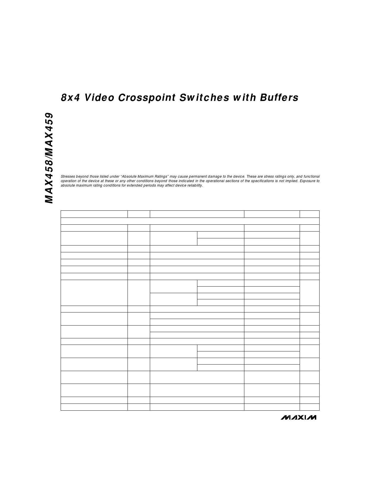
8x4 Video Crosspoint Switches with Buffers
ABSOLUTE MAXIMUM RATINGS
Total Supply Voltage (VCC to VEE) .........................................12V
Positive Supply Voltage (VCC to GND).....................................6V
Negative Supply Voltage (VEE to GND) ...................................6V
Analog Input/Output Voltage ...........(VCC + 0.3V) to (VEE - 0.3V)
Digital Input Voltage ...................................(VCC + 0.3V) to -0.3V
Duration of Output Short Circuit to GND (Note 1) ......Continuous
Continuous Power Dissipation
Plastic DIP (derate 17mW/°C above +70°C) ..............1333mW
PLCC (derate 13mW/°C above +70°C) ......................1067mW
Operating Temperature Ranges
MAX45_C_ _ ........................................................0°C to +70°C
MAX45_E_ _......................................................-40°C to +85°C
Junction Temperature ......................................................+150°C
Storage Temperature Range .............................-65°C to +160°C
Lead Temperature (soldering, 10sec) .............................+300°C
Note 1: Outputs may be shorted to any supply pin or ground as long as package power dissipation ratings are not exceeded.
Stresses beyond those listed under “Absolute Maximum Ratings” may cause permanent damage to the device. These are stress ratings only, and functional
operation of the device at these or any other conditions beyond those indicated in the operational sections of the specifications is not implied. Exposure to
absolute maximum rating conditions for extended periods may affect device reliability.
ELECTRICAL CHARACTERISTICS
(VCC = +5V, VEE = -5V, -2V ≤ VIN ≤ +2V, output load resistor (RL) = 150Ω, TA = TMIN to TMAX, unless otherwise noted.
Typical values are at TA = +25°C.)
PARAMETER
SYMBOL
CONDITIONS
MIN TYP MAX
STATIC SPECIFICATIONS
Input Voltage Range
-2
+2
Input Offset Voltage
VOS Any channel
TA = +25°C
TA = TMIN to TMAX
5
15
20
Input Offset Voltage Match
∆VOS VIN = 0V (Note 2)
3
10
Power-Supply Rejection Ratio
PSRR VS = ±4.75V to ±5.25V
50
60
On Input Bias Current
IIN
VIN = 0V, input programmed to one output
±1
±5
On Input Resistance
RIN Input programmed to one output
0.50 5.0
Input Capacitance
CIN Input channel on or off
7
DC Voltage Gain Accuracy
Output Voltage Swing
Enabled Output Resistance
Disabled Output Resistance
VOUT
ROUT
ROUT
MAX458 (Note 3)
MAX459 (Note 4)
TA = +25°C
TA = TMIN to TMAX
TA = +25°C
TA = TMIN to TMAX
VIN = 1kHz sine wave
VIN = 10MHz sine wave
MAX458
MAX459
0.1
0.5
1.0
0.1
1.0
2.0
±2
±3
0.05
4.0
0.25 1.0
0.70 1.0
Disabled Output Capacitance
Positive Power-Supply Current
Negative Power-Supply Current
COUT
ICC
IEE
VIN = 0V,
all amplifiers enabled
VIN = 0V,
all amplifiers enabled
TA = +25°C
TA = TMIN to TMAX
TA = +25°C
TA = TMIN to TMAX
12
60
75
85
50
100
50
65
75
40
90
Positive Supply Current in
Shutdown
15
26
UNITS
V
mV
mV
dB
µA
MΩ
pF
%
V
Ω
MΩ
kΩ
pF
mA
mA
mA
Negative Supply Current in
Shutdown
Logic Input High Voltage
Logic Input Low Voltage
VIH
(Note 5)
VIL
(Note 5)
7
12
mA
2.0
V
0.8
V
2 _______________________________________________________________________________________
Share Link: 