74LVQ74 Ver la hoja de datos (PDF) - STMicroelectronics
Número de pieza
componentes Descripción
Fabricante
74LVQ74 Datasheet PDF : 11 Pages
| |||
74LVQ74
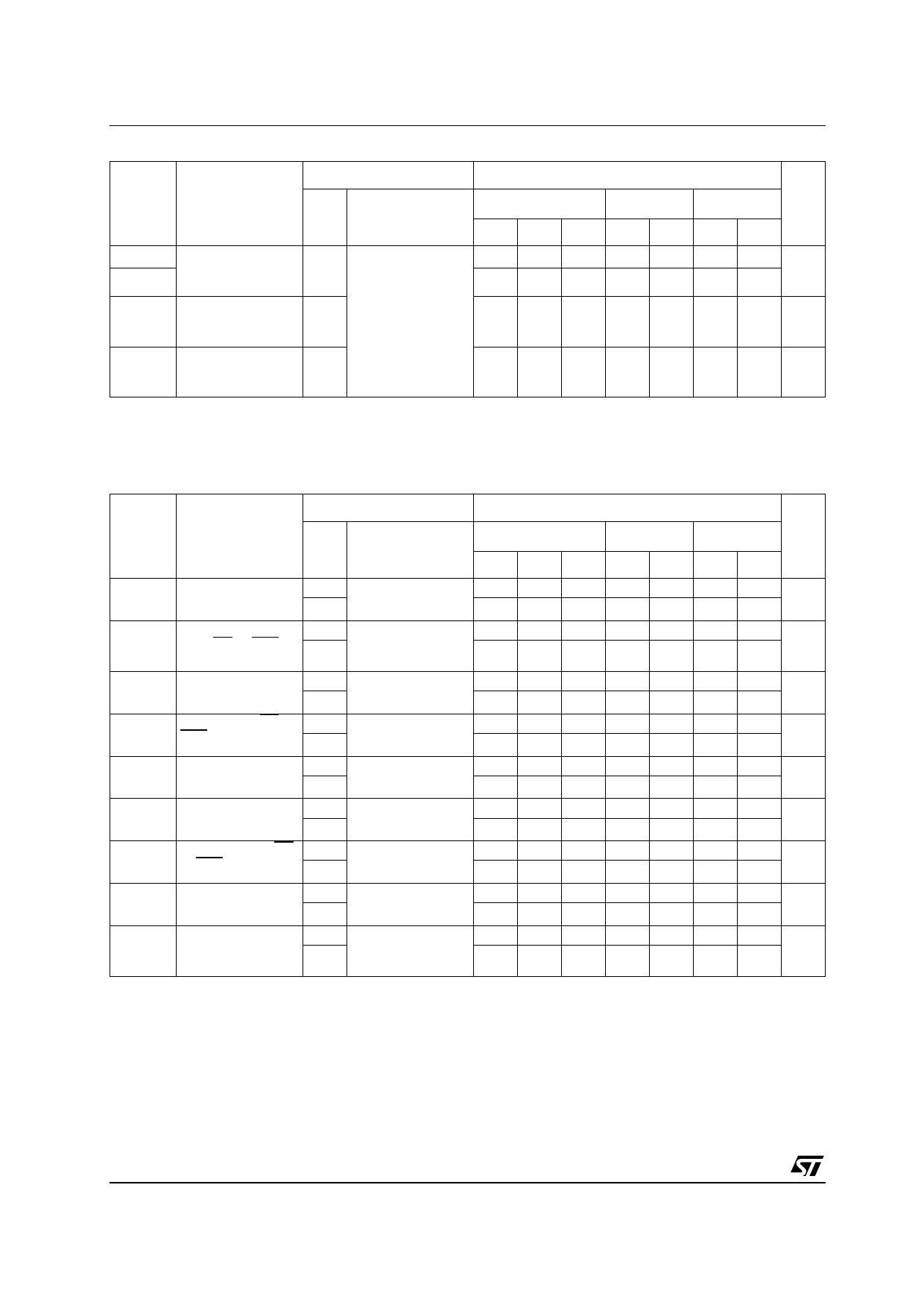
DYNAMIC SWITCHING CHARACTERISTICS
Test Condition
Value
Symbol
Parameter
VCC
(V)
TA = 25°C
-40 to 85°C -55 to 125°C Unit
Min. Typ. Max. Min. Max. Min. Max.
VOLP Dynamic Low
0.2 0.8
Voltage Quiet
3.3
V
VOLV Output (note 1, 2)
-0.8 -0.2
VIHD Dynamic High
3.3
2
V
Voltage Input (note
CL = 50 pF
1, 3)
VILD Dynamic Low
3.3
Voltage Input (note
1, 3)
0.8
V
1) Worst case package.
2) Max number of outputs defined as (n). Data inputs are driven 0V to 3.3V, (n-1) outputs switching and one output at GND.
3) Max number of data inputs (n) switching. (n-1) switching 0V to 3.3V. Inputs under test switching: 3.3V to threshold (VILD), 0V to threshold
(VIHD), f=1MHz.
AC ELECTRICAL CHARACTERISTICS (CL = 50 pF, RL = 500 Ω, Input tr = tf = 3ns)
Test Condition
Value
Symbol
Parameter
VCC
(V)
TA = 25°C
-40 to 85°C -55 to 125°C Unit
Min. Typ. Max. Min. Max. Min. Max.
tPLH Propagation Delay 2.7
tPHL Time CK to Q
3.3(*)
7.7 12.0
6.3 9.0
14.0
10.5
16.0
ns
12.0
tPLH Propagation Delay 2.7
tPHL
Time PR or CLR to
Q
3.3(*)
6.9 12.0
5.8 9.0
14.0
10.5
16.0
ns
12.0
tw Pulse Width CK , 2.7
HIGH or LOW
3.3(*)
4.0 1.5
4.0
5.0
ns
3.0 1.5
3.0
4.0
tw(L) Pulse Width PR or 2.7
CLR, LOW
3.3(*)
4.0 1.5
4.0
5.0
ns
3.0 1.5
3.0
4.0
ts
Setup Time D to CK 2.7
HIGH or LOW
3.3(*)
4.0 -0.2
4.0
5.0
ns
3.0 -0.2
3.0
4.0
th Hold Time D to CK 2.7
HIGH or LOW
3.3(*)
2.0 0.2
2.0
2.0
ns
2.0 0.2
2.0
2.0
tREM
Recovery Time PR 2.7
or CLR to Q
3.3(*)
1.0 -1.0
1.0
1.0
ns
1.0 -1.0
1.0
1.0
fMAX Maximum Clock
Frequency
2.7
3.3(*)
100 200
100
80
MHz
120 250
120
100
tOSLH
tOSHL
Output To Output
Skew Time
(note1, 2)
2.7
3.3(*)
0.2 1.0
1.0
1.0
0.2 1.0
1.0
1.0 ns
1) Skew is defined as the absolute value of the difference between the actual propagation delay for any two outputs of the same device switch-
ing in the same direction, either HIGH or LOW (tOSLH = |tPLHm - tPLHn|, tOSHL = |tPHLm - tPHLn|)
2) Parameter guaranteed by design
(*) Voltage range is 3.3V ± 0.3V
4/11
Share Link: 