A8511 Ver la hoja de datos (PDF) - Allegro MicroSystems
NГєmero de pieza
componentes DescripciГіn
Fabricante
A8511 Datasheet PDF : 24 Pages
| |||
A8511
2 MHz, 4 ChannelГ—150 mA WLED/RGB Driver
with Output Disconnect
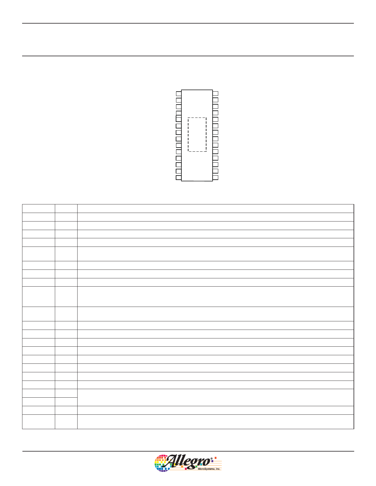
Pin-out Diagram
BIAS 1
DGND 2
DIM 3
SW 4
SW 5
SW 6
OVP 7
CAP 8
AGND 9
ISET 10
VTI 11
VTO 12
LED1 13
LED2 14
28 EN
27 SEL2
26 SEL1
25 PGND
24 PGND
23 PGND
PAD
22 NC
21 VIN
20 COMP
19 FSET
18 OUT
17 LED4
16 LED3
15 LGND
Terminal List Table
Number Name
Function
1
BIAS Output of internal 6 V bias supply. Decouple with a 0.1 ОјF ceramic capacitor to DGND.
2
DGND Digital signal ground. Connect AGND, DGND, LGND, PGND, and PAD using star ground connection.
3
4, 5, 6
DIM Sets ILED by adjusting the ISET to ILEDx current gain, AISET . When DIM = VIL , AISET = 960 and when DIM=VIH , AISET = 240.
SW DMOS switch drain node. Tie these three pins together on the PCB.
7
OVP
To enable overvoltage protection, connect this pin through a resistor to the CAP pin. The default OVP level, with 0 О© resistor,
is 19.5 V. External resistor can set OVP up to 38 V.
8
CAP Input connection for output disconnect switch.
9
AGND Analog signal ground. Connect AGND, DGND, LGND, PGND, and PAD using star ground connection.
10
ISET Sets the 100% current level through LED strings. Set by value of RISET connected between ISET and AGND.
ISET voltage override. Sets the ISET voltage when VTI < 1.23 V. Tie directly to VTO pin to disable this feature. This pin can
11
VTI be used for LED current thermal derating or external analog LED current control. See the Typical Application Circuits section
for additional information.
12
VTO
2.46 V output voltage. Use this voltage to bias an external NTC resistor or as a DAC reference. This pin can be used as a
logic high signal for the SEL and DIM pins.
13,14,16,17 LEDX LED current sinks.
15
LGND Power ground for LED current sinks. Connect AGND, DGND, LGND, PGND, and PAD using star ground connection.
18
OUT Output connection for output disconnect switch. Connect LED common connection to this pin.
19
FSET Connect RFSET between FSET and AGND to set boost switching frequency.
20
COMP Sets boost loop compensation. Connect external compensation capacitor between COMP and AGND for boost converter stability.
21
VIN Input supply for the device. Decouple with a 0.1 ОјF ceramic capacitor.
22
NC Not connected internally. It is recommended to connect this pin to external ground.
23, 24, 25 PGND Power ground. Connect AGND, DGND, LGND, PGND, and PAD using star ground connection.
26
SEL1
SEL1 and SEL2 together select which LED strings are enabled. See Functional Description section.
27
SEL2
28
EN Enable and PWM LED current control. Apply logic-level PWM for PWM-controlled dimming mode.
–
PAD
Exposed thermal pad. Connect AGND, DGND, LGND, PGND, and PAD using star ground connection. Connect to PCB
copper layer for enhanced heat dissipation.
8511-DS
Allegro MicroSystems, Inc.
4
115 Northeast Cutoff
Worcester, Massachusetts 01615-0036 U.S.A.
1.508.853.5000; www.allegromicro.com
Share Link: 