BUK9606-75B Ver la hoja de datos (PDF) - NXP Semiconductors.
Número de pieza
componentes Descripción
Fabricante
BUK9606-75B Datasheet PDF : 13 Pages
| |||
Nexperia
BUK9606-75B
N-channel TrenchMOS logic level FET
Table 6. Characteristics …continued
Symbol
Parameter
Conditions
Source-drain diode
VSD
source-drain voltage IS = 40 A; VGS = 0 V; Tj = 25 °C;
see Figure 15
trr
reverse recovery time IS = 20 A; dIS/dt = -100 A/µs;
Qr
recovered charge
VGS = -10 V; VDS = 25 V; Tj = 25 °C
350
ID
(A)
300
250
5
4
10
200
150
100
50
0
0
2
4
03ng84
VGS = 3 V
2.4
6
8
10
VDS (V)
8
RDSon
(mΩ)
7
6
5
4
0
Min Typ Max Unit
-
0.85 1.2 V
-
68
-
ns
-
176 -
nC
03ng83
5
10
15
VGS (V)
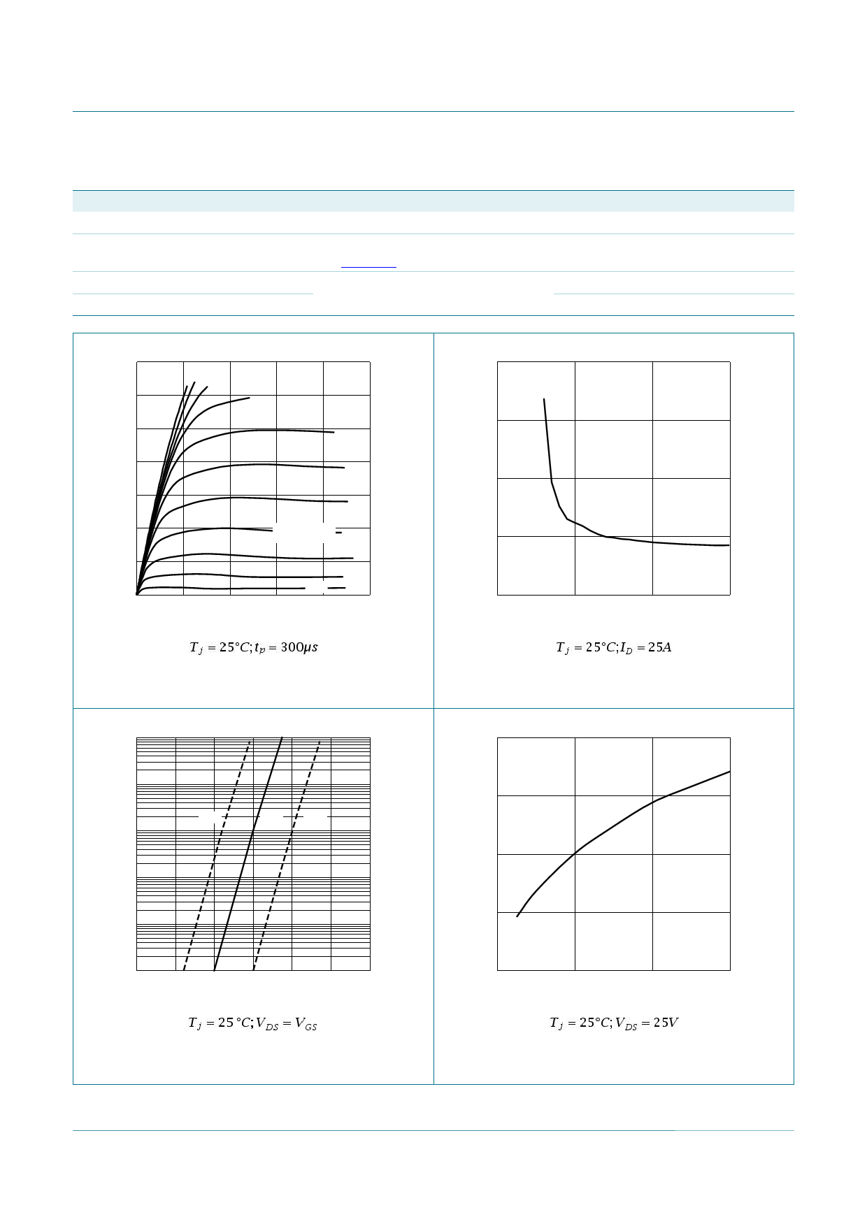
Fig 5. Output characteristics: drain current as a
Fig 6. Drain-source on-state resistance as a function
function of drain-source voltage; typical values
of gate-source voltages; typical values
10−1
ID
(A)
10−2
10−3
10−4
03ng53
min
typ
max
200
gfs
(S)
150
100
03ng81
50
10−5
10−6
0
1
2
3
VGS (V)
0
0
20
40
60
ID (A)
Fig 7. Sub-threshold drain current as a function of
gate-source voltage
Fig 8. Forward transconductance as a function of
drain current; typical values
BUK9606-75B
Product data sheet
All information provided in this document is subject to legal disclaimers.
Rev. 4 — 20 July 2011
© Nexperia B.V. 2017. All rights reserved
6 of 13
Share Link: 