CM1233 Ver la hoja de datos (PDF) - ON Semiconductor
N├║mero de pieza
componentes Descripci├│n
Fabricante
CM1233 Datasheet PDF : 13 Pages
| |||
CM1233
The PicoGuard XS Architecture Advantages
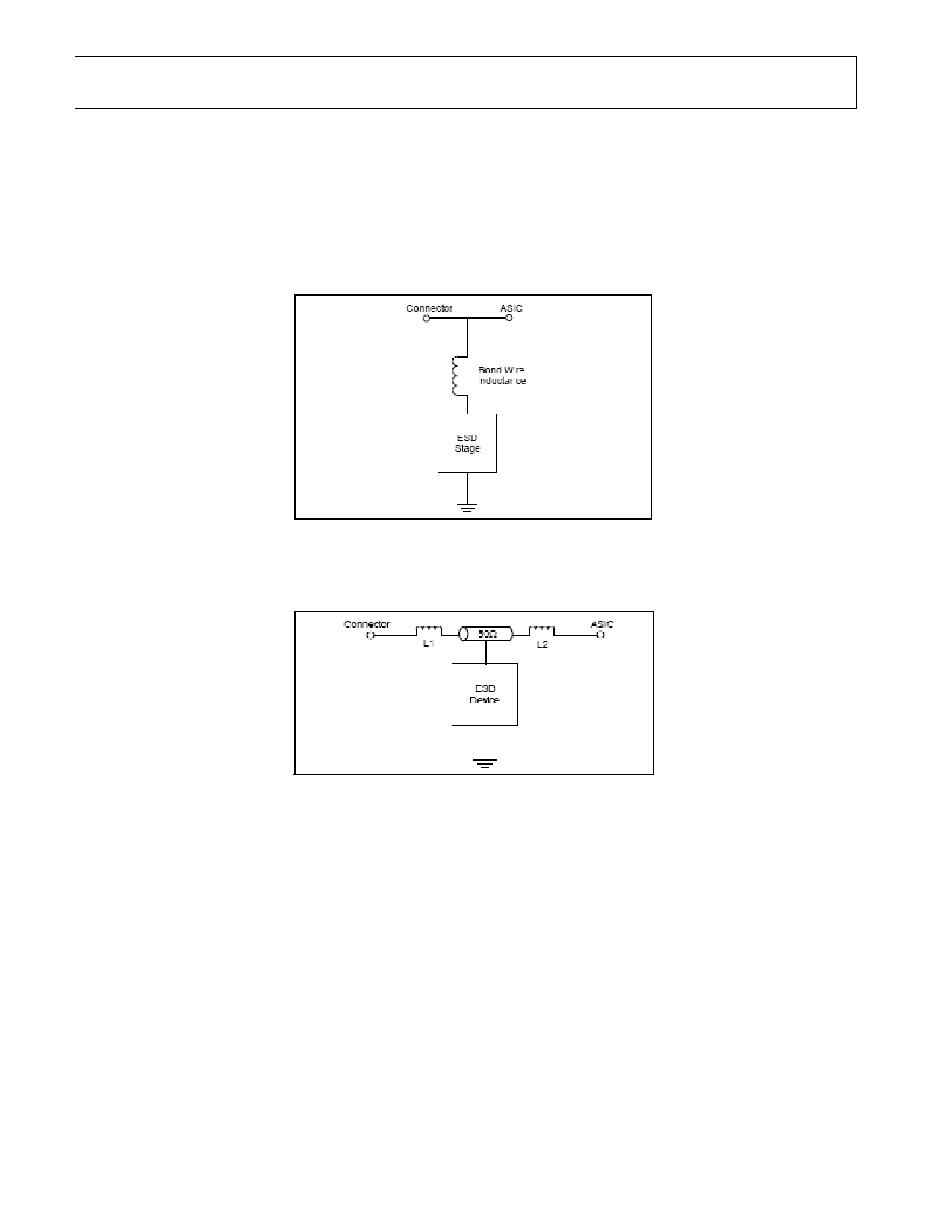
Figure 2 illustrates a standard ESD protection device. The inductor element represents the parasitic inductance
arising from the bond wire and the PCB trace leading to the ESD protection diodes.
Figure 2. Standard ESD Protection Model
Figure 3 illustrates one of the channels. Similarly, the inductor elements represent the parasitic inductance arising
from the bond wire and PCB traces leading to the ESD protection diodes as well.
Figure 3. CM1233 PicoGuard XS ESD Protection Model
Rev. 2 | Page 4 of 13 | www.onsemi.com
Share Link: 