CY7C006A-20JXC(2013) Ver la hoja de datos (PDF) - Cypress Semiconductor
NГғmero de pieza
componentes DescripciГіn
Fabricante
CY7C006A-20JXC Datasheet PDF : 22 Pages
| |||
CY7C006A
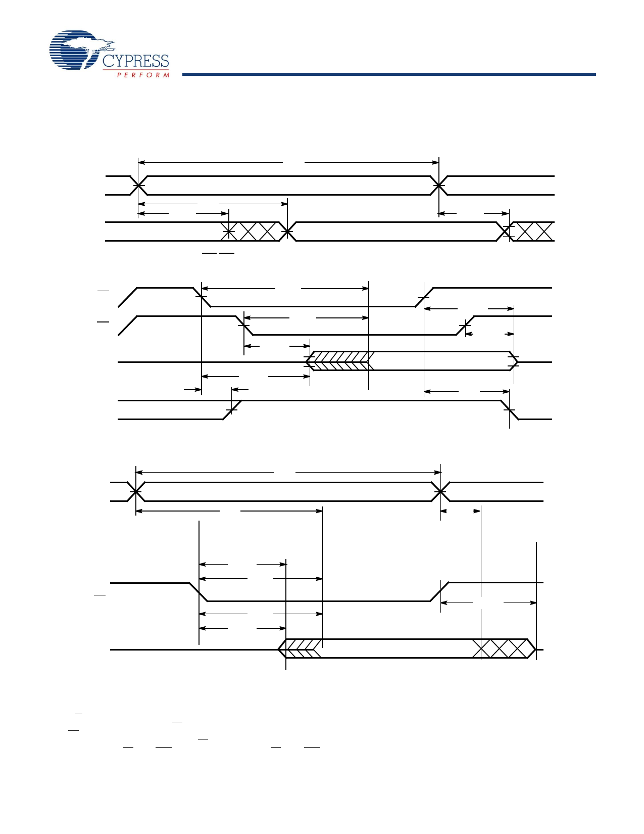
Switching Waveforms (continued)
Figure 7. Write Cycle No. 1: R/W Controlled Timing [21, 22, 23, 24]
tWC
ADDRESS
OE
tHZOE[26]
CE [25]
R/W
DATA OUT
tAW
tSA
tPWE[24]
NOTE 27
tHZWE[26]
tHA
tLZWE
NOTE 27
DATA IN
tSD
tHD
ADDRESS
CE [25]
R/W
Figure 8. Write Cycle No. 2: CE Controlled Timing [21, 22, 23, 28]
tWC
tAW
tSA
tSCE
tHA
DATA IN
tSD
tHD
Notes
21. R/W or CE must be HIGH during all address transitions.
22. A write occurs during the overlap (tSCE or tPWE) of a LOW CE or SEM.
23. tHA is measured from the earlier of CE or R/W or (SEM or R/W) going HIGH at the end of write cycle.
24.
If OE is LOW during a R/W controlled
placed on the bus
specified tPWE.
for
the
required
tSD.
write cycle, the write
If OE is HIGH during
paunlsRe/Wwicdothntmroullsetdbwertihteeclaycrglee,rtohfistPreWqEuoirre(mtHeZnWt Edo+etsSnDo) ttoapapllloywanthdethI/eOwdrriitveeprsultsoetucarnn
off
be
and data to
as short as
be
the
25. To access RAM, CE = VIL, SEM = VIH.
26. Transition is measured В±500 mV from steady state with a 5-pF load (including scope and jig). This parameter is sampled and not 100% tested.
27. During this period, the I/O pins are in the output state, and input signals must not be applied.
28. If the CE or SEM LOW transition occurs simultaneously with or after the R/W LOW transition, the outputs remain in the high-impedance state.
Document Number: 38-06045 Rev. *G
Page 11 of 22
Share Link: 