CY7C63001C-XC Ver la hoja de datos (PDF) - Cypress Semiconductor
Número de pieza
componentes Descripción
Fabricante
CY7C63001C-XC Datasheet PDF : 28 Pages
| |||
7.0 Absolute Maximum Ratings
Storage Temperature ................................. –65°C to +150°C
Ambient Temperature with Power Applied ...... –0°C to +70°C
Supply Voltage on VCC Relative to VSS ......... –0.5V to +7.0V
DC Input Voltage................................... –0.5V to +VCC+0.5V
DC Voltage Applied to Outputs in High-Z state –0.5V to +VCC+0.5V
Max. Output Current into Port 1 Pins ...........................60 mA
Max. Output Current into Non-Port 1 Pins .................. 10 mA
Power Dissipation .....................................................300 mW
Static Discharge Voltage ...........................................>2000V
Latch-up Current[1].................................................. >200 mA
CY7C63001C
CY7C63101C
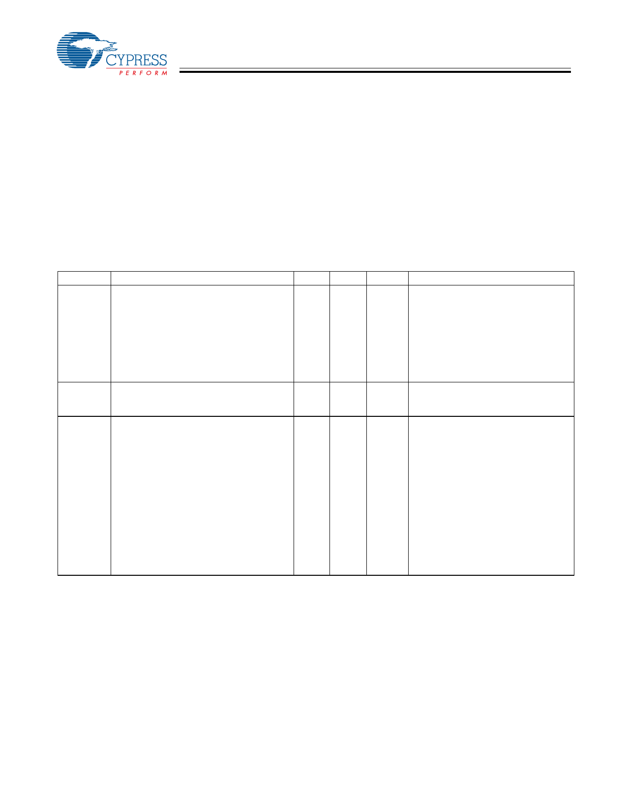
8.0
ICC
ISB1
ISB2
VPP
tstart
twatch
Electrical Characteristics fOSC = 6 MHz; Operating Temperature = 0 to 70°C, VCC = 4.0 to 5.25 volts
Parameter
Min Max Units
Conditions
General
VCC Operating Supply Current
Supply Current—Suspend Mode
25
mA
20
µA Resonator off, D– > Voh min[2]
Supply Current—Start-up Mode
4
mA
Programming Voltage (disabled)
–0.4 0.4
V
Resonator Start-up Interval
256
µs Ceramic resonator
Watch Dog Timer Period
7.168 8.192 ms
tVCCS
Power On Reset
VCC Slew
0.010 1000
ms Linear ramp on VCC pin to VCC[3, 4]
USB Interface
Voh
Static Output High
2.8 3.6
V
15kΩ ± 5% to Gnd[5,6]
Vol
Static Output Low
0.3
V See Notes 5 and 6
Vdi
Differential Input Sensitivity
0.2
V |(D+)–(D–)|, and Figure 6-23
Vcm
Differential Input Common Mode Range
0.8 2.5
V Figure 6-23
Vse
Single Ended Receiver Threshold
0.8 2.0
V
Cin
Transceiver Input Capacitance
20
pF D+ to Vss; D- to Vss
Ilo
Data Line (D+, D–) Leakage
–10 10
µA 0 V <(D+, D–)<3.3 V, Hi-Z State
Rpu1
Rpu2
External Bus Pull-up Resistance, D– pin
External Bus Pull-up Resistance, D– pin
1.425 1.575
7.425 7.575
kΩ 1.5 kΩ ± 5% to 3.3V supply
kΩ 7.5 kΩ ± 1% to Vcc[7]
Rpd
External Bus Pull-down Resistance
14.25 15.75 kΩ 15 kΩ ± 5%
Notes:
1. All pins specified for >200 mA positive and negative injection, except P1.0 is specified for >50 mA negative injection.
2. Cext at VCC or Gnd, Port 0 and Port1 at VCC.
3. Part powers up in suspend mode, able to be reset by USB Bus Reset.
4. POR may re-occur whenever VCC drops to approximately 2.5V.
5. Level guaranteed for range of VCC = 4.35V to 5.25V.
6. With Rpu1 of 1.5 KW±5% on D– to 3.3V regulator.
7. Maximum matched capacitive loading allowed on D+ and D– (including USB cable and host/hub) is approximately 230 pF.
Document #: 38-08026 Rev. *B
Page 20 of 28
Share Link: 