HIP6602CB Ver la hoja de datos (PDF) - Intersil
Número de pieza
componentes Descripción
Fabricante
HIP6602CB Datasheet PDF : 9 Pages
| |||
HIP6602
Absolute Maximum Ratings
Supply Voltage (VCC) . . . . . . . . . . . . . . . . . . . . . . . . . . . . . . . . .15V
Supply Voltage (PVCC) . . . . . . . . . . . . . . . . . . . . . . . . . VCC + 0.3V
BOOT Voltage (VBOOT - VPHASE) . . . . . . . . . . . . . . . . . . . . . . .15V
Input Voltage (VPWM) . . . . . . . . . . . . . . . . . . . . . . GND - 0.3V to 7V
UGATE. . . . . . . . . . . . . . . . . . . . . . VPHASE - 0.3V to VBOOT + 0.3V
LGATE . . . . . . . . . . . . . . . . . . . . . . . . .GND - 0.3V to VPVCC + 0.3V
ESD Rating
Human Body Model (Per MIL-STD-883 Method 3015.7) . . . . .3kV
Machine Model (Per EIAJ ED-4701 Method C-111) . . . . . . .200V
Thermal Information
Thermal Resistance (Note 1)
θJA (°C/W)
SOIC Package . . . . . . . . . . . . . . . . . . . . . . . . . . . . .
68
Maximum Junction Temperature (Plastic Package) . . . . . . . . 150°C
Maximum Storage Temperature Range . . . . . . . . . . -65°C to 150°C
Maximum Lead Temperature (Soldering 10s) . . . . . . . . . . . . . 300°C
(SOIC - Lead Tips Only)
Operating Conditions
Ambient Temperature Range. . . . . . . . . . . . . . . . . . . . . 0°C to 85°C
Maximum Operating Junction Temperature. . . . . . . . . . . . . . . 125°C
Supply Voltage, VCC . . . . . . . . . . . . . . . . . . . . . . . . . . . . 12V ±10%
Supply Voltage Range PVCC . . . . . . . . . . . . . . . . . . . . . 5V to 12V
CAUTION: Stresses above those listed in “Absolute Maximum Ratings” may cause permanent damage to the device. This is a stress only rating and operation of the
device at these or any other conditions above those indicated in the operational sections of this specification is not implied.
NOTE:
1. θJA is measured with the component mounted on a high effective thermal conductivity test board in free air. See Tech Brief TB379 for details.
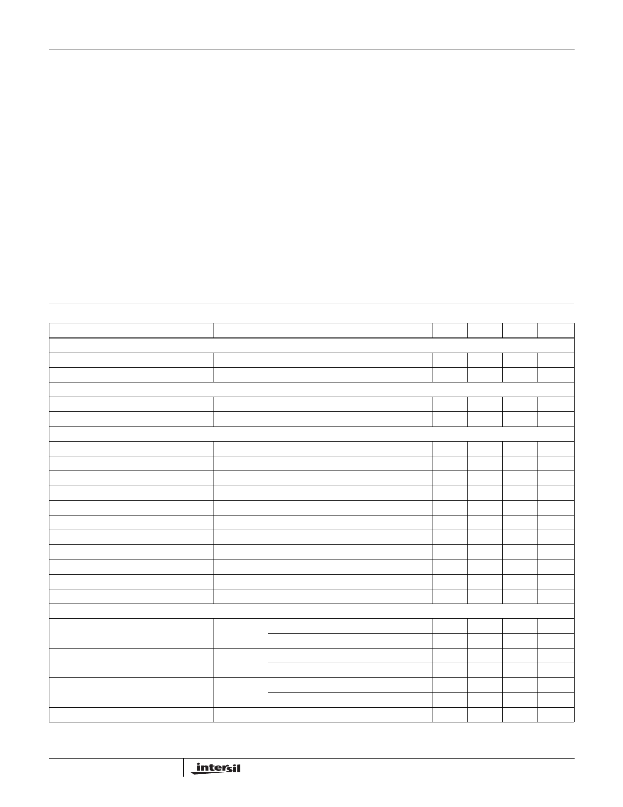
Electrical Specifications Recommended Operating Conditions, Unless Otherwise Noted
PARAMETER
SYMBOL
TEST CONDITIONS
VCC SUPPLY CURRENT
Bias Supply Current
Power Supply Current
POWER-ON RESET
IVCC
IPVCC
fPWM = 500kHz, VPVCC = 12V
fPWM = 500kHz, VPVCC = 12V
VCC Rising Threshold
VCC Falling Threshold
PWM INPUT
Input Current
PWM Rising Threshold
PWM Falling Threshold
UGATE Rise Time
LGATE Rise Time
UGATE Fall Time
LGATE Fall Time
UGATE Turn-Off Propagation Delay
LGATE Turn-Off Propagation Delay
Shutdown Window
IPWM
VPWM = 0 or 5V (See Block Diagram)
VPVCC = 12V
VPVCC = 12V
TRUGATE VPVCC = VVCC = 12V, 3nF Load
TRLGATE VPVCC = VVCC = 12V, 3nF Load
TFUGATE VPVCC = VVCC = 12V, 3nF Load
TFLGATE VPVCC = VVCC = 12V, 3nF Load
TPDLUGATE VPVCC = VVCC = 12V, 3nF Load
TPDLLGATE VPVCC = VVCC = 12V, 3nF Load
Shutdown Holdoff Time
OUTPUT
Upper Drive Source Impedance
Upper Drive Sink Impedance
Lower Drive Source Current
Lower Drive Sink Impedance
RUGATE
RUGATE
ILGATE
RLGATE
VVCC = 12V, VPVCC = 5V
VVCC = VPVCC = 12V
VVCC = 12V, VPVCC = 5V
VVCC = VPVCC = 12V
VVCC = 12V, VPVCC = 5V
VVCC = VPVCC = 12V
VVCC = 12V, VPVCC = 5V or 12V
MIN TYP MAX UNITS
-
3.7
5.0
mA
-
2.0
4.0
mA
9.7
9.95 10.4
V
9.0
9.2
9.5
V
-
500
-
µA
3.45
3.6
-
V
-
1.45 1.55
V
-
20
-
ns
-
50
-
ns
-
20
-
ns
-
20
-
ns
-
30
-
ns
-
20
-
ns
1.4
-
3.6
V
-
230
-
ns
-
1.7
3.0
Ω
-
3.0
5.0
Ω
-
2.3
4.0
Ω
-
1.1
2.0
Ω
400
580
-
mA
500
730
-
mA
-
1.6
4.0
Ω
4
Share Link: 