MAX189BCPA Ver la hoja de datos (PDF) - Maxim Integrated
Número de pieza
componentes Descripción
Fabricante
MAX189BCPA Datasheet PDF : 20 Pages
| |||
+5V, Low-Power, 12-Bit Serial ADCs
____________Applications Information
Connection to Standard Interfaces
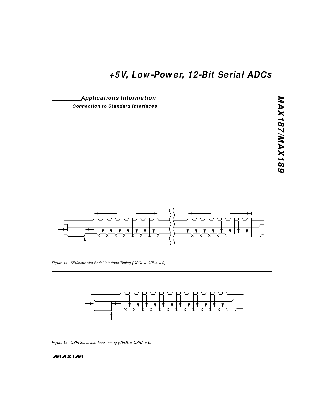
The MAX187/MAX189 serial interface is fully compatible
with SPI, QSPI, and Microwire standard serial
interfaces.
If a serial interface is available, set the CPU’s serial
interface in master mode so the CPU generates the ser-
ial clock. Choose a clock frequency up to 2.5MHz.
1. Use a general-purpose I/O line on the CPU to pull CS
low. Keep SCLK low.
2. Wait the for the maximum conversion time specified
before activating SCLK. Alternatively, look for a
DOUT rising edge to determine the end of
conversion.
3. Activate SCLK for a minimum of 13 clock cycles. The
first falling clock edge will produce the MSB of the
DOUT conversion. DOUT output data transitions on
SCLK’s falling edge and is available in MSB-first for-
mat. Observe the SCLK to DOUT valid timing charac-
teristic. Data can be clocked into the µP on SCLK’s
rising edge.
4. Pull CS high at or after the 13th falling clock edge. If
CS remains low, trailing zeros are clocked out after
the LSB.
5. With CS = high, wait the minimum specified time, tCS,
before launching a new conversion by pulling CS
low. If a conversion is aborted by pulling CS high
before the conversions end, wait for the minimum
acquisition time, tACQ, before starting a new
conversion.
Data can be output in 1-byte chunks or continuously, as
shown in Figure 8. The bytes will contain the result of
the conversion padded with one leading 1, and trailing
0s if SCLK is still active with CS kept low.
1ST BYTE READ
2ND BYTE READ
SCLK
CS
HI-Z
tCONV
HI-Z
DOUT
MSB D10 D9 D8 D7 D6 D5
D4
D3 D2 D1 LSB
EOC
Figure 14. SPI/Microwire Serial Interface Timing (CPOL = CPHA = 0)
SCLK
CS
HI-Z
DOUT
tCONV
HI-Z
MSB D10 D9 D8 D7 D6 D5 D4 D3 D2 D1 LSB
EOC
Figure 15. QSPI Serial Interface Timing (CPOL = CPHA = 0)
______________________________________________________________________________________ 15
Share Link: 