LTC1315CG Ver la hoja de datos (PDF) - Linear Technology
Número de pieza
componentes Descripción
Fabricante
LTC1315CG Datasheet PDF : 12 Pages
| |||
LTC1314/LTC1315
ELECTRICAL CHARACTERISTICS VDD = 5V, VCCIN = 5V, VPPIN = 12V, TA = 25°C unless otherwise specified.
SYMBOL
VOH
VOL
VG-VDD
tON
tOFF
t1
t2
t3
t4
t5
t6
t7
PARAMETER
SHDN Output High Voltage
SHDN Output Low Voltage
Gate Voltage Above Supply
Turn-On Time, DRV3 and DRV5
Turn-Off Time, DRV3 and DRV5
Delay + Rise Time
Delay + Rise Time
Delay + Rise Time
Delay + Fall Time
Delay + Fall Time
Delay + Fall Time
Output Turn-On Delay
CONDITIONS
VPPOUT = VCCIN, 0V or Hi-Z, ILOAD = 400µA q
VPPOUT = VPPIN, ISINK = 400µA
q
VDRV3 or VDRV5
q
CGATE = 1000pF, Time for VGATE > VDD + 1V
CGATE = 1000pF, Time for VGATE < 0.5V
VPPOUT = GND to VCCIN, VPPIN = 0V, Note 1
VPPOUT = GND to VPPIN (Note 1)
VPPOUT = VCCIN to VPPIN (Note 1)
VPPOUT = VPPIN to VCCIN (Note 3)
VPPOUT = VPPIN to GND (Note 2)
VPPOUT = VCCIN to GND, VPPIN = 0V (Note 2)
VPPOUT = Hi-Z to VPPIN or VCCIN (Notes 1, 6)
LTC1314/LTC1315
MIN TYP MAX
3.5
0.4
6
7
13
50
150 500
3
10
30
5
15
50
5
15
50
5
15
50
2
6
20
15
50
150
10
25
100
5
15
50
UNITS
V
V
V
µs
µs
µs
µs
µs
µs
µs
µs
µs
The q denotes specifications which apply over the full operating
temperature range.
Note 1: To 90% of the final value, COUT = 0.1µF, ROUT = 2.9k.
Note 2: To 10% of the final value, COUT = 0.1µF, ROUT = 2.9k.
Note 3: To 50% of the initial value, COUT = 0.1µF, ROUT = 2.9k.
Note 4: Measured current data is per channel.
Note 5: Input logic low equal to 0V, high equal to 5V.
Note 6: VPPIN = 0V when switching from Hi-Z to VCCIN.
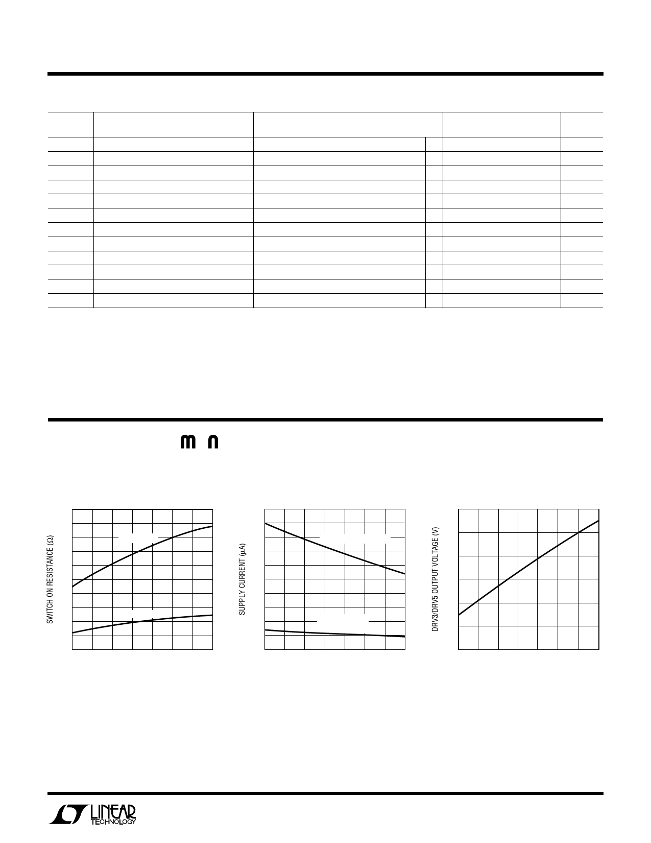
TYPICAL PERFORMANCE CHARACTERISTICS
Switch On Resistance vs
Temperature
3.0
2.7
2.4
VCC SWITCH
2.1
1.8
1.5
1.2
0.9
VPP SWITCH
0.6
0.3
0
–50 –30 –10 10 30 50
TEMPERATURE (°C)
70 90
1314/15 G01
Supply Current vs Temperature
75
70
65
VPPOUT = VPPIN = 12V
60
55
50
45
40
35
VPPOUT = VCCIN
VPPIN = 12V
30
25
–50 –30 –10 10 30 50 70 90
TEMPERATURE (°C)
1314/15 G02
DRV3/DRV5 Output Voltage vs
Temperature
14.2
14.0
13.8
13.6
13.4
13.2
13.0
–50 –30
–10 10 30 50
TEMPERATURE (°C)
70 90
1314/15 G03
3
Share Link: 