43631 Ver la hoja de datos (PDF) - Linear Technology
Número de pieza
componentes Descripción
Fabricante
43631 Datasheet PDF : 24 Pages
| |||
LT4363
Applications Information
VIN
12V
D1*
SMAJ58CA
Q2
SI7461DP
R7
10k
5 VCC
Q1
IRLR2908
RSNS
10mΩ
D2
1N5245
R3
15V
10Ω
C1
47nF
4
3
GATE SNS
2
OUT
FB 1
VOUT
12V, 3A
CLAMPED
AT 16V
R1
57.6k
R2
4.99k
6 SHDN
8 UV
7 OV
*DIODES INC.
LT4363DE-2
GND
9
ENOUT 11
TMR
FLT 10
12
CTMR
0.1µF
4363 F07
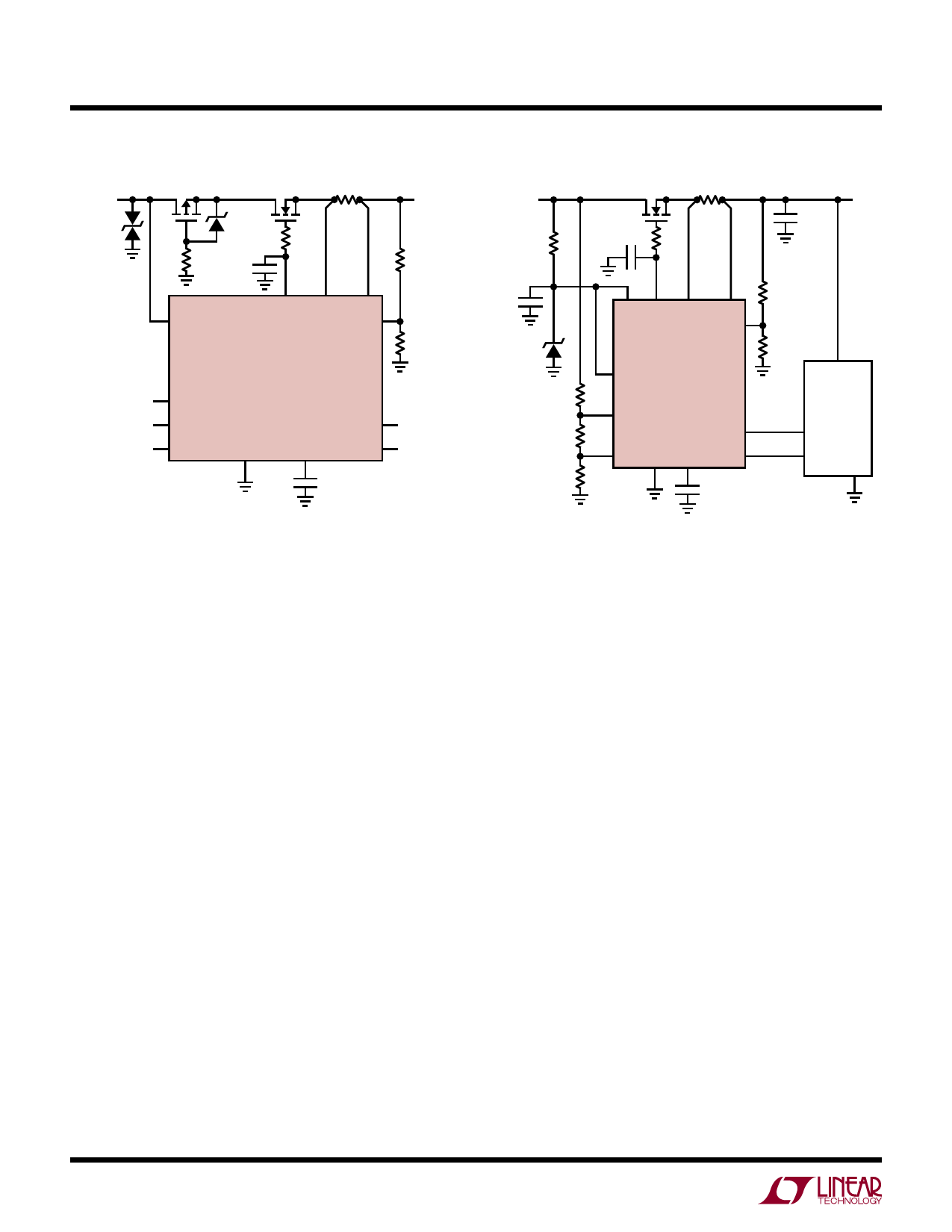
Figure 7. Overvoltage Regulator with P-channel MOSFET
Reverse Input Protection
Shutdown
The LT4363 can be shut down to a low current mode when
the voltage at the SHDN pin is pulled below the shutdown
threshold of 0.4V. The quiescent current drops down to
7µA with internal circuitry turned off.
The SHDN pin can be pulled up to 100V or below GND by
up to 60V without damage. Leaving the pin open allows
an internal current source to pull it up and turn on the part
while clamping the pin to 2.2V. The leakage current at the
pin should be limited to no more than 1µA if no pull up
device is used to help turn it on.
Supply Transient Protection
The LT4363 is tested to operate to 80V and guaranteed to
be safe from damage up to 100V. Nevertheless, voltage
transients above 100V may cause permanent damage.
During a short-circuit condition, the large change in cur-
rent flowing through power supply traces and associated
wiring can cause inductive voltage transients which could
exceed 100V. To minimize the voltage transients, the power
trace parasitic inductance should be minimized by using
wide traces. A small RC filter, in Figure 8, at the VCC pin
will clamp the voltage spikes.
VIN
R7
1k
Q1
RSNS
FDB33N25 10mΩ
C1
47nF
R3
10Ω
CL**
22µF
VOUT
C2
0.1µF
D1*
SMAJ58A
R4
374k
R5
90.9k
R6
10k
54 3
VCC GATE SNS
2
R1
100k
OUT
FB 1
6 SHDN
LT4363DE-2
R2
4.99k
8 UV
ENOUT 11
VCC
DC/DC
CONVERTER
SHDN
7 OV
GND TMR
FLT 10
FAULT
GND
9
12
4363 F08
CTMR
47nF *DIODES INC.
**SANYO 25CE22GA
Figure 8. Overvoltage Regulator with Input Voltage Detection
Another way to limit transients above 100V at the VCC
pin is to use a Zener diode and a resistor, D1 and R7 in
Figure 8. The Zener diode limits the voltage at the pin while
the resistor limits the current through the diode to a safe
level during the surge. However, D1 can be omitted if the
filtered voltage, due to R7 and C1, at the VCC pin is below
100V. The inclusion of R7 in series with the VCC pin will
increase the minimum required voltage at VIN due to the
extra voltage drop across it. This voltage drop is due to the
supply current of the LT4363 and the leakage current of D1.
A total bulk capacitance of at least 22µF low ESR electro-
lytic is required close to the source pin of MOSFET Q1. In
addition, the bulk capacitance should be at least 10 times
larger than the total ceramic bypassing capacitor on the
input of the DC/DC converter.
Layout Considerations
To achieve accurate current sensing, Kelvin connection
to the current sense resistor (RSNS in Figure 8) is recom-
mended. The minimum trace width for 1 oz copper foil is
0.02" per amp to ensure the trace stays at a reasonable
temperature. 0.03" per amp or wider is recommended.
Note that 1oz copper exhibits a sheet resistance of about
530µΩ/square. Small resistances can cause large errors in
high current applications. Noise immunity will be improved
16
For more information www.linear.com/LT4363
4363fb
Share Link: 