LVT22V10 Ver la hoja de datos (PDF) - Philips Electronics
Número de pieza
componentes Descripción
Fabricante
LVT22V10 Datasheet PDF : 20 Pages
| |||
Philips Semiconductors
3V high speed, universal PLD device
Product specification
LVT22V10
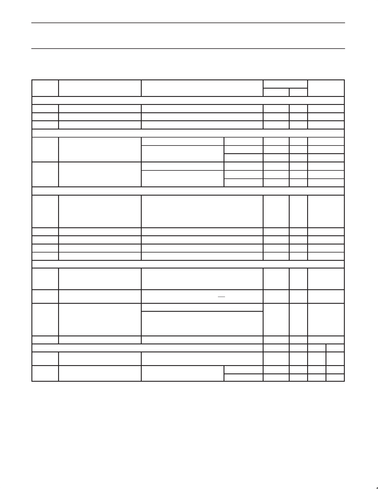
DC ELECTRICAL CHARACTERISTICS
Over operating ranges.
SYMBOL
PARAMETER
TEST CONDITIONS1
LIMITS
MIN MAX
UNIT
Input voltage
VIL
Low
VIH
High
VI
Clamp
Output voltage
VCC = MIN
VCC = MAX
VCC = MIN, IIN = –18mA
0.8
V
2.0
V
–1.2
V
VOH
High-level output voltage
VOL
Low-level output voltage
Input current
VCC = MIN to MAX, VI = VIH or VIL IOH = –100 µA VCC–0.2
V
VCC = MIN, VI = VIH or VIL
IOH = –16mA
2.0
IOH = –5.5 mA
2.4
V
V
VCC = MIN to MAX, VI = VIH or VIL IOL = 100µA
0.2
V
VCC = MIN, VI = VIH or VIL
IOL = 32 mA
IOL = 16 mA
0.5
V
0.4
V
IIL
Low
IIH
High
II
Max input current
II
Pin 1 (program)
IBHL
Bus hold low sustaining current2
IBHH
Bus hold high sustaining current3
IBHLO
Bus hold low overdrive current4, 9
IBHHO
Bus hold high overdrive current5, 9
Output current
VCC = MAX, VIN = 0.0V
VCC = MAX, VIN = VCC
VCC = MAX, VIN = 5.5V
VCC = MAX, VIN = 5.5V
VCC = 3V, VI = 0.8V
VCC = 3V, VI = 2V
VCC = 3.6V
VCC = 3.6V
–10
µA
10
µA
10
µA
20
µA
75
µA
–75
µA
500
µA
–500
µA
IOFF
Output off current
VCC = 0V, VI or VO = 0 to 4.5V
±10
µA
IEX
Current into an output in high state
when VO > VCC
VO = 5.5V, VCC = 3.0V
±100
µA
IPU/PD
Power-up/down 3-State output
current8
VCC <1.2V; VO = 0.5V to VCC;
VI = GND or VCC; OE/OE = X
100
µA
VCC = MAX
IOZH
Output leakage6
VIN = VIL or VIH, VOUT = 5.5V
10
µA
IOZL
Output leakage6
ISC
Short circuit7
VIN = VIL or VIH, VOUT =0V
VOUT = 0.5V
–10
µA
–30 –220
mA
ICC
VCC supply current
VCC = 3.6V, Outputs enabled, VI = VCC or GND; IO = 0
170
mA
Ground/VCC Bounce
MIN
TYP MAX UNIT
VOHV
Maximum dynamic VOH
VCC = 3.0V, 25°C,
CL = 50pF (including jig capacitance)
2.2
2.3
V
VOLP
Maximum dynamic VOL
VCC = 3.3V, 25°C, CL = 50pF
(including jig capacitance)
LVT22V10-7
LVT22V10B7
0.7 1.1
V
1.0 1.1
V
NOTES:
1. These are absolute values with respect to device ground and all overshoots due to system or tester noise are included.
2. The bus hold circuit can sink at least the minimum low sustaining current at VIL MAX. IBHL should be measured after lowering VIN to GND
and then raising it to VIL MAX.
3. The bus hold circuit can source at least the minimum high sustaining current at VIH MIN. IBHL should be measured after raising VIN to VCC
and then lowering it to VIH MIN.
4. An external driver must source at least IBHLO to switch this node from low to high.
5. An external driver must sink at least IBHHO to switch this node from high to low.
6. I/O pin leakage is the worst case of IOZX or IIX (where X = H or L).
7. No more than one output should be tested at a time. Duration of the short-circuit test should not exceed one second. VOUT = 0.5V has been
chosen to avoid test problems caused by tester ground degradation.
8. This parameter is valid for any VCC between 0V and 1.2 V with a transition time up to 10 mS. From VCC = 1.2 to VCC = 3.3V ±0.3V a
transition time of 100 µS is permitted. X = Don’t care.
9. These parameters are not 100% tested, but are evaluated at initial characterization and at any time the design is modified where input
current may be affected.
1998 Feb 10
5
Share Link: 