MT88L85AP Ver la hoja de datos (PDF) - Mitel Networks
Número de pieza
componentes Descripción
Fabricante
MT88L85AP Datasheet PDF : 20 Pages
| |||
Advance Information
MT88L85
Pin Description
Pin #
24 28
Name
8,9 3,5, NC No Connection.
17
10,11
16,
20,
25
Functional Description
Description
Receiver Section
The MT88L85 Integrated DTMF Transceiver consists
of a high performance DTMF receiver with an
internal gain setting amplifier and a DTMF generator,
which employs a burst counter to synthesize precise
tone bursts and pauses. A call progress mode can
be selected so that frequencies within the specified
passband can be detected. The adaptive micro
interface allows microcontrollers, such as the
68HC11, 80C51 and TMS370C50, to access the
MT88L85 internal registers.
Power Down
The MT88L85 provides enhanced power down
functionality to facilitate minimization of supply
current consumption. DTMF transmitter and receiver
circuit blocks may be independently powered down
via register control. When asserted, the RxEN
control bit powers down all analog and digital
circuitry associated solely with the DTMF and Call
Progress receiver. The TOUT control bit is used to
disable the transmitter and put all circuitry
associated only with the DTMF transmitter in power
down mode. With the TOUT control bit asserted, the
TONE output pin is held in a high impedance
(floating) state. When both power down control bits
are asserted, circuits utilized by both the DTMF
transmitter and receiver are also powered down.
This includes the crystal oscillators, and the VRef
generator. In addition, the IRQ , TONE output and
DATA pins are held in a high impedance state.
Finally, the whole device is put in a power down state
when the PWDN pin is asserted.
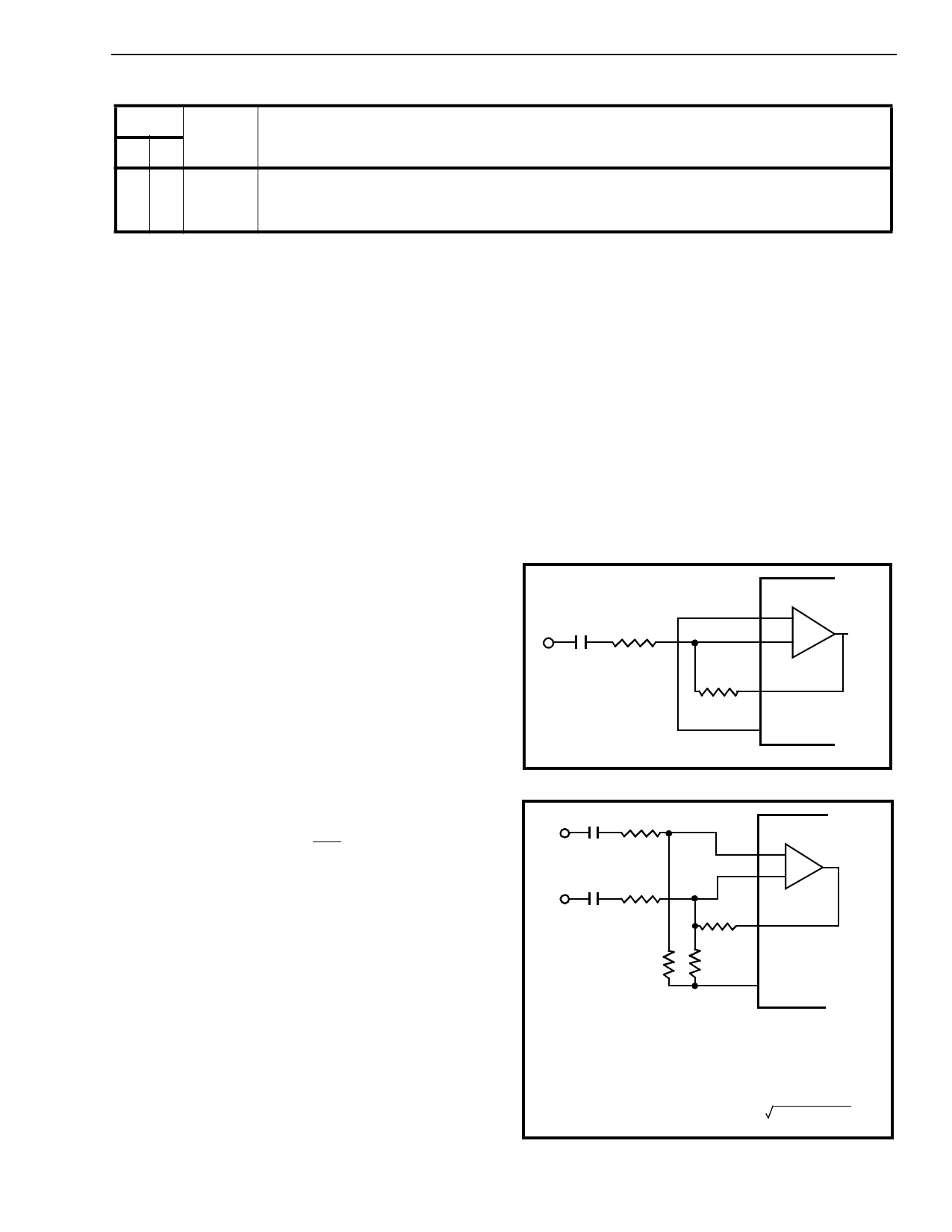
Input Configuration
The input arrangement of the MT88L85 provides a
differential-input operational amplifier as well as a
bias source (VRef), which is used to bias the inputs at
VDD/2. Provision is made for connection of a
feedback resistor to the op-amp output (GS) for gain
adjustment. In a single-ended configuration, the
input pins are connected as shown in Figure 3.
Figure 4 shows the necessary connections for a
differential input configuration.
Separation of the low and high group tones is
achieved by applying the DTMF signal to the inputs
of two sixth-order switched capacitor bandpass
filters, the bandwidths of which correspond to the low
and high group frequencies (see Table 1). The filters
also incorporate notches at 350 Hz and 440 Hz for
exceptional dial tone rejection. Each filter output is
followed by a single order switched capacitor filter
section, which smooths the signals prior to limiting.
Limiting is performed by high-gain comparators
which are provided with hysteresis to prevent
detection of unwanted low-level signals. The outputs
of the comparators provide full rail logic swings at
the frequencies of the incoming DTMF signals.
MT88L85
IN+
C
RIN
IN-
VOLTAGE GAIN
(AV) = RF / RIN
RF
GS
VRef
Figure 3 - Single-Ended Input Configuration
C1
R1
MT88L85
IN+
C2
R4
R3
IN-
R5
GS
R2
VRef
DIFFERENTIAL INPUT AMPLIFIER
C1 = C2 = 10 nF
R1 = R4 = R5 = 100 kΩ
R2 = 60kΩ, R3 = 37.5 kΩ
R3 = (R2R5)/(R2 + R5)
VOLTAGE GAIN
(AV diff) - R5/R1
INPUT IMPEDANCE
(ZINdiff) = 2 R12 + (1/ωC)2
Figure 4 - Differential Input Configuration
4-73
Share Link: 