NCP1608 Ver la hoja de datos (PDF) - ON Semiconductor
Número de pieza
componentes Descripción
Fabricante
NCP1608 Datasheet PDF : 24 Pages
| |||
NCP1608
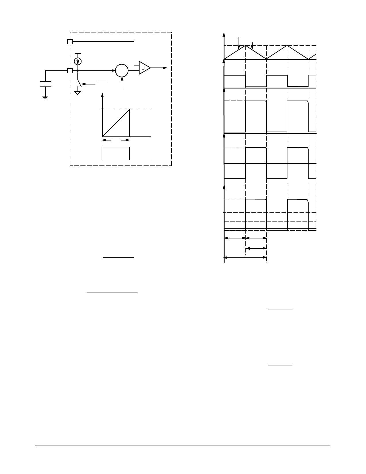
Control
Ct
VDD
Icharge
VControl
+
PWM
−
+
ton
DRV
Ct(offset)
VCt
VCt(off)
VControl − Ct(offset)
IL
IL(peak)
MOSFET Conduction
Diode Conduction
0A
DRV
Vdrain
0V
Vout
ton
DRV
Figure 31. On Time Generation
VControl varies with the rms input voltage and output
load, which naturally satisfies Equation 1. The on time is
constant during the ac line cycle if the values of
compensation components are sufficient to filter out the
Vout ripple. The maximum on time of the controller occurs
when VControl is at the maximum. The Ct capacitor is sized
to ensure that the required on time is reached at maximum
output power and the minimum input voltage condition.
The maximum on time is calculated using Equation 7:
ton(MAX)
+
Ct
@ VCt(MAX)
Icharge
(eq. 7)
Combining Equation 7 with Equation 1, results in
Equation 8:
Ct
w
2 @ Pout @ L @ Icharge
h @ VacLL 2 @ VCt(MAX)
(eq. 8)
To calculate the minimum Ct value:
VCt(MAX) = 4.775 V (minimum value),
Icharge = 297 mA (maximum value), and VacLL is the
minimum rms input voltage.
Off Time Sequence
In CrM operation, the on time is constant during the ac
line cycle and the off time varies with the instantaneous
input voltage. When the inductor current reaches zero, the
drain voltage (Vdrain in Figure 27) resonates towards Vin.
Measuring Vdrain is a way to determine when the inductor
current reaches zero. To measure the high voltage Vdrain
directly is generally not economical or practical. Instead,
a winding is added to the boost inductor. This winding,
called the Zero Current Detection (ZCD) winding,
provides a scaled representation of the inductor voltage
that is sensed by the controller. Figure 32 shows waveforms
of ideal CrM operation using a ZCD winding.
VZCD(WIND)
0V
VZCD(WIND),off
0V
VZCD(WIND),on
VZCD
VCL(POS)
VZCD(ARM)
VZCD(TRIG)
VCL(NEG)
0V
ton
tdiode
toff
TSW
Figure 32. Ideal CrM Waveforms Using a ZCD
Winding
The voltage induced on the ZCD winding during the switch
on time (VZCD(WIND),on) is calculated using Equation 9:
VZCD(WIND),on
+
−Vin
NB : NZCD
(eq. 9)
Where Vin is the instantaneous input voltage and NB:NZCD
is the turns ratio of the boost winding to the ZCD winding.
The voltage induced on the ZCD winding during the
switch off time (VZCD(WIND),off) is calculated using
Equation 10:
VZCD(WIND),off
+
Vout
NB :
* Vin
NZCD
(eq. 10)
When the inductor current reaches zero, the ZCD pin
voltage (VZCD) follows the ZCD winding voltage
(VZCD(WIND)) and begins to decrease and ring towards zero
volts. The NCP1608 detects the falling edge of VZCD and
turns the driver on. To ensure that a ZCD event is not
inadvertently detected, the NCP1608 logic verifies that
VZCD exceeds VZCD(ARM) and then senses that VZCD
decreases to less than VZCD(TRIG) (Figure 33).
http://onsemi.com
14
Share Link: 