NE5539D Ver la hoja de datos (PDF) - Philips Electronics
Número de pieza
componentes Descripción
Fabricante
NE5539D Datasheet PDF : 14 Pages
| |||
Philips Semiconductors
High frequency operational amplifier
Product data
NE/SE5539
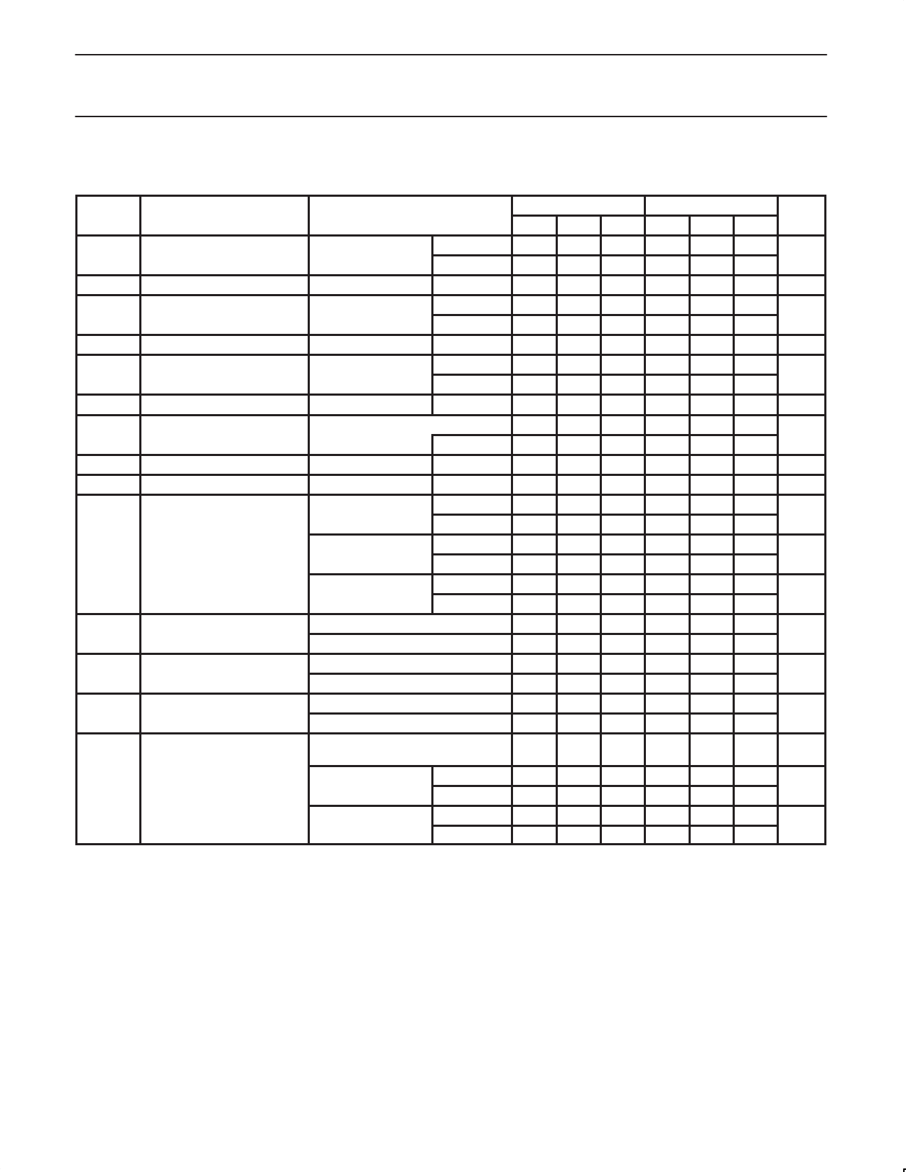
DC ELECTRICAL CHARACTERISTICS
VCC = ±8 V, Tamb = 25 °C; unless otherwise specified.
SYMBOL
PARAMETER
TEST CONDITIONS
VOS
∆VOS/∆T
IOS
∆IOS/∆T
IB
∆IB/∆T
CMRR
RIN
ROUT
VOUT
ICC+
ICC–
PSRR
AVOL
Input offset voltage
Input offset current
Input bias current
Common mode rejection ratio
Input impedance
Output impedance
Output voltage swing
Positive supply current
Negative supply current
Power supply rejection ratio
Large signal voltage gain
VO = 0 V;
RS = 100 Ω
Over temp.
Tamb = 25 °C
Over temp.
Tamb = 25 °C
Over temp.
Tamb = 25 °C
F = 1 kHz; RS = 100 Ω; VCM ±1.7 V
Over temp.
RL = 150 Ω to GND
and 470 Ω to –VCC
+Swing
–Swing
RL = 25 Ω to GND
Over temp.
+Swing
–Swing
RL = 25 Ω to GND
Tamb = 25 °C
+Swing
–Swing
VO = 0 V, R1 = ∞; Over temp.
VO = 0 V, R1 = ∞; Tamb = 25 °C
VO = 0 V, R1 = ∞; Over temp.
VO = 0 V, R1 = ∞; Tamb = 25 °C
∆VCC = ±1 V; Over temp.
∆VCC = ±1 V; Tamb = 25 °C
VO = +2.3 V, –1.7 V;
RL = 150 Ω to GND, 470 Ω to –VCC
VO = +2.3 V, –1.7 V; Over temp.
RL = 2 Ω to GND Tamb = 25 °C
VO = +2.5 V, –2.0 V; Over temp.
RL = 2 Ω to GND Tamb = 25 °C
SE5539
MIN TYP MAX
2
5
2
3
5
0.1
3
0.1
1
0.5
6
25
5
13
10
70
80
70
80
100
10
+2.3 +3.0
–1.5 –2.1
+2.5 +3.1
–2.0 –2.7
14
18
14
17
11
15
11
14
300 1000
46
60
48
53
58
NE5539
UNITS
MIN TYP MAX
mV
2.5
5
5
µV/°C
µA
2
0.5
nA/°C
µA
5
20
10
nA/°C
70
80
dB
100
kΩ
10
Ω
+2.3 +2.7
V
–1.7 –2.2
V
V
mA
14
18
mA
11
15
µV/V
200 1000
47
52
57
dB
dB
47
52
57
dB
2002 Jan 25
4
Share Link: 