S6B0723 Ver la hoja de datos (PDF) - Samsung
Número de pieza
componentes Descripción
Fabricante
S6B0723 Datasheet PDF : 71 Pages
| |||
S6B0723 PRELIMINARY SPEC. VER. 0.9
65 COM / 132 SEG DRIVER & CONTROLLER FOR STN LCD
SYSTEM CONTROL
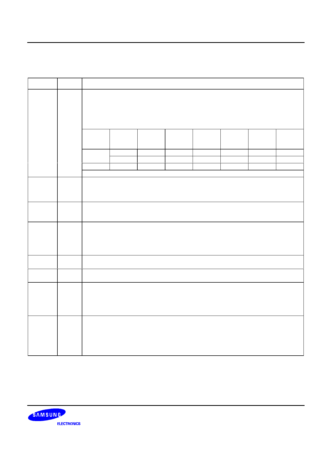
Table 5. System Control Pins Description
Name
MS
I/O
Description
Master / slave mode select input
Master makes some signals for display, and slave gets them. This is for display
synchronization.
− MS = "H": master mode
− MS = "L": slave mode
The following table depends on the MS status.
I
MS
CLS
OSC
circuit
Power
supply
circuit
CL
M
FR
DISP
H
H
Enabled Enabled Output Output Output Output
L
Disabled Enabled Input Output Output Output
L
-
Disabled Disabled Input
Input Output Input
CLS
CL
M
FRS
FR
DISP
INTRS
Built-in oscillator circuit enable / disable select pin
I
− CLS = “H”: enable
− CLS = “L”: disable (external display clock input to CL pin)
Display clock input / output pin
I/O When the S6B0723 is used in master/slave mode (multi-chip), the CL pins must be
connected each other.
LCD AC Signal input / output pin
When the S6B0723 is used in master/slave mode (multi-chip), the M pins must be
I/O connected each other.
− MS = “H”: output
− MS = “L”: input
O
Static driver segment output pin
This pin is used together with the FR pin.
O
Static driver common output pin
This pin is used together with the FRS pin.
LCD display blanking control input / output
When S6B0723 is used in master/slave mode (multi-chip), the DISP pins must be
I/O connected each other.
− MS = “H”: output
− MS = “L”: input
Internal resistor select pin
This pin selects the resistors for adjusting V0 voltage level and is valid only in master
I
operation.
− INTRS = "H": use the internal resistors.
− INTRS = "L": use the external resistors.
V0 voltage is controlled by VR pin and external resistive divider.
9
Share Link: 