TA8492PG Ver la hoja de datos (PDF) - Toshiba
Número de pieza
componentes Descripción
Fabricante
TA8492PG Datasheet PDF : 14 Pages
| |||
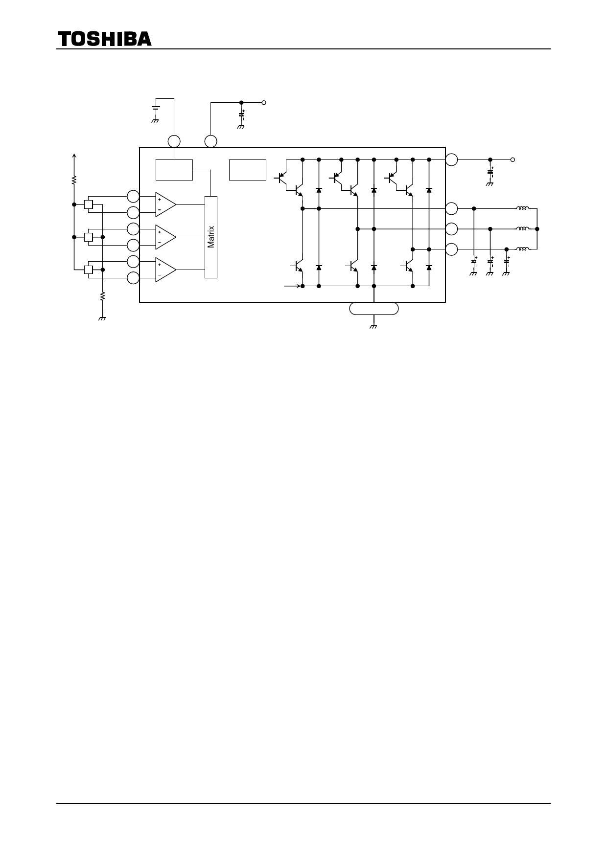
Application Circuit
VCC
R1
3ST 3
Ha+
Ha−
Hb+
Hb−
Hc+
Hc−
7
6
11
10
9
8
R1
FRC
12 V
C1
14 VCC
TSD
TA8492P/PG
16 VS
2 La
15 Lb
1 Lc
12 V
C2
C3
4, 5, 12, 13 GND
Note:
Utmost care is necessary in the design of the output, VCC, VM, and GND lines since the IC may be destroyed
by short-circuiting between outputs, air contamination faults, or faults due to improper grounding, or by
short-circuiting between contiguous pins.
10
2006-3-2
Share Link: 