LB1695M Ver la hoja de datos (PDF) - SANYO -> Panasonic
Número de pieza
componentes Descripción
Fabricante
LB1695M Datasheet PDF : 7 Pages
| |||
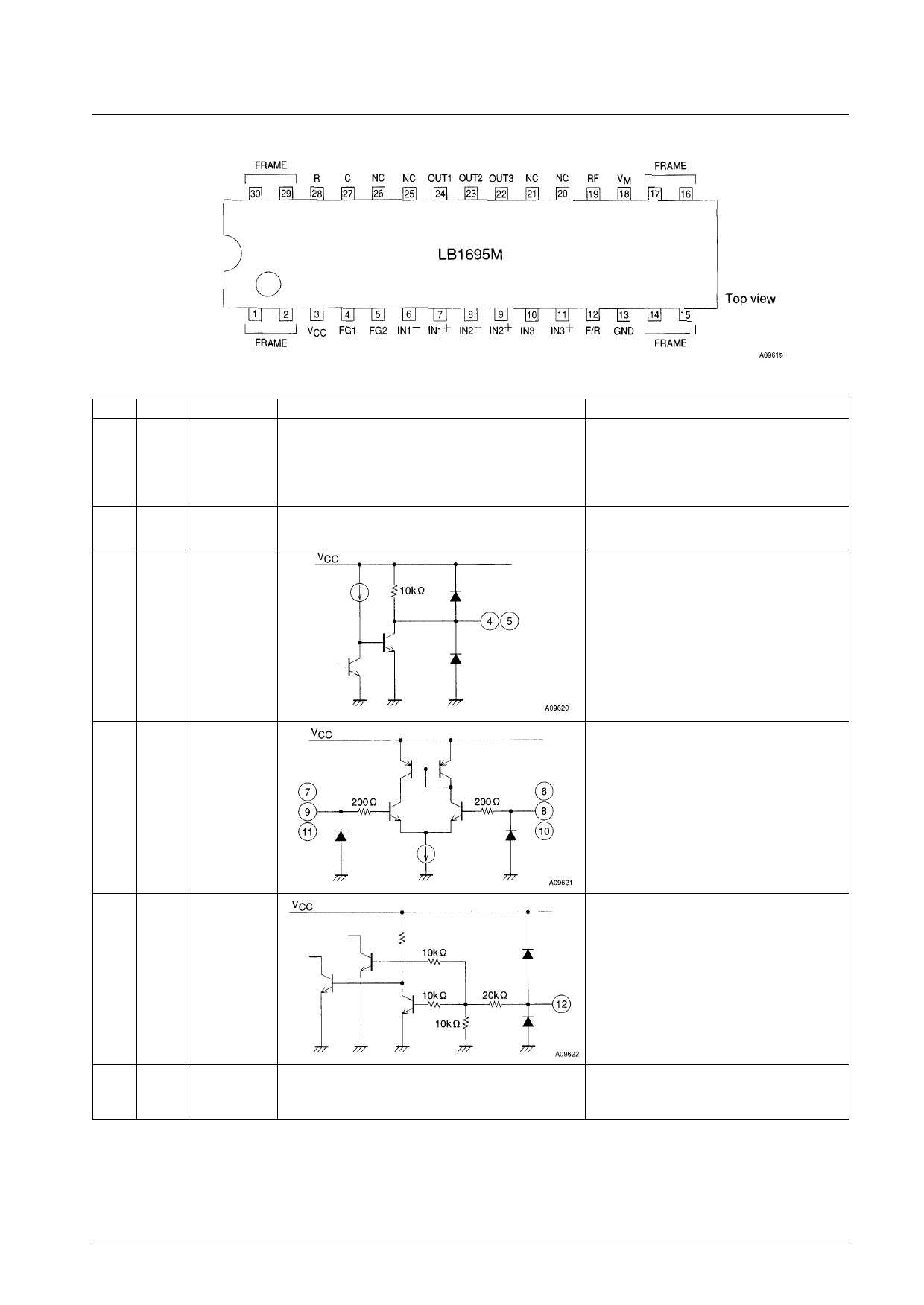
Pin Assignment
LB1695M
Pin Functions
Pin No. Symbol Pin voltage (V)
1, 2,
14, 15,
FRAME
16, 17,
29, 30
3
VCC
4
FG1
5
FG2
6
IN1–
7
IN1+
8
IN2–
1.5 V min
9
IN2+ VCC – 1.8 V max
10
IN3–
11
IN3+
12
F/R
0.0 V min
VCC max
13
GND
Equivalent circuit
Pin function
• Pins provided for heat dissipation. These pins must
be electrically open.
• Power supply for blocks other than the output
block.
• Speed pulse output 1
A pull-up resistor is built in.
• Speed pulse output 2
A pull-up resistor is built in.
• Hall inputs. The logic high state is when IN+ > IN–.
• Forward reverse control
• Ground for blocks other than the output block.
The RF pin voltage will be the lowest potential
taken on be the output transistors.
Continued on next page.
No. 5802-3/7
Share Link: 