UPD16835AGS-BGG Ver la hoja de datos (PDF) - NEC => Renesas Technology
Número de pieza
componentes Descripción
Fabricante
UPD16835AGS-BGG Datasheet PDF : 32 Pages
| |||
µPD16835A
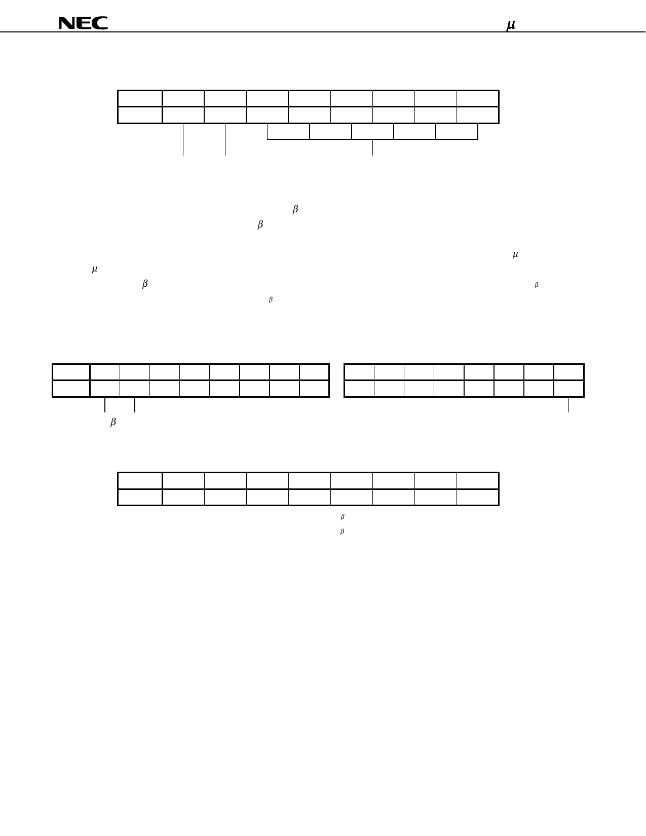
Table 5-11. 5th Byte Data Configuration (Standard data)
Bit
Data
D7
0 or 1
D6
0 or 1
D5
0 or 1
D4
0 or 1
D3
0 or 1
D2
0 or 1
D1
0 or 1
D0
0 or 1
Rotation direction ENABLE
Number of pulses
<6th and 7th bytes>
The 6th and 7th bytes select the pulse cycle of the β channel and which of the two reference voltages, created in
the initial mode, is to be used (CURRENT SETβ).
The pulse cycle is specified using 15 bits : bits D0 (least significant bit) to D7 of the 6th byte, and bits D0 to D6
(most significant bit) of the 7th byte. The pulse cycle can be set to a value in the range of 0.25 to 8191.75 µs in units
of 0.25 µs (with a 4-MHz clock).
CURRENT SETβ is specified by bit D7 of the 7th byte. When this bit is “0”, reference voltage 1 (EVRβ1) is
selected; when it is “1”, reference voltage 2 (EVRβ2) is selected. For further information, refer to the description of the
7th byte of the initial data.
Table 5-12. 7th Byte Data Configuration (Standard data) Table 5-13. 6th Byte Data Configuration (Standard data)
Bit
Data
D7 D6 D5 D4 D3 D2 D1 D0
0 or 1 0 or 1 0 or 1 0 or 1 0 or 1 0 or 1 0 or 1 0 or 1
D7 D6 D5 D4 D3 D2 D1 D0
0 or 1 0 or 1 0 or 1 0 or 1 0 or 1 0 or 1 0 or 1 0 or 1
CURRENT SETβ Most significant bit
Least significant bit
(Reference) 7th Byte Data Configuration for Initial Data
Bit
D7
D6
D5
D4
D3
Data
0 or 1 0 or 1 0 or 1 0 or 1 0 or 1
Remark Bits D4 to D7 : Reference voltage 2 (EVR β2)
Bits D0 to D3 : Reference voltage 1 (EVR β1)
D2
0 or 1
D1
0 or 1
D0
0 or 1
<8th byte>
The 8th byte is checksum data. Normally, the sum of the 8-byte data is 00H.
If the sum is not 00H because data transmission is abnormal, the stepping operation is inhibited and the
checksum output pin (EXT pin) is held at “L”.
18
Data Sheet S15973EJ1V0DS
Share Link: 