LT1721IS Ver la hoja de datos (PDF) - Linear Technology
Número de pieza
componentes Descripción
Fabricante
LT1721IS
Linear Technology
LT1721IS Datasheet PDF : 28 Pages
| |||
LT1720/LT1721
APPLICATIONS INFORMATION
and 100µV/°C baseline uncertainty. Switching delay is
less than 15ns and the minimum sampling window width
for full power response is 30ns.
The input waveform is presented to the diode bridge
switch, the output of which feeds the LT1227 wideband
amplifier. The LT1720 comparators, triggered by the sample
command, generate phase-opposed outputs. These sig-
nals are level shifted by the transistors, providing comple-
mentary bipolar drive to switch the bridge. A skew
compensation trim ensures bridge-drive signal simulta-
neity within 1ns. The AC balance corrects for parasitic
capacitive bridge imbalances. A DC balance adjustment
trims bridge offset.
The trim sequence involves grounding the input via 50Ω
and applying a 100kHz sample command. The DC balance
is adjusted for minimal bridge ON vs OFF variation at the
output. The skew compensation and AC balance adjust-
ments are then optimized for minimum AC disturbance in
the output. Finally, unground the input and the circuit is
ready for use.
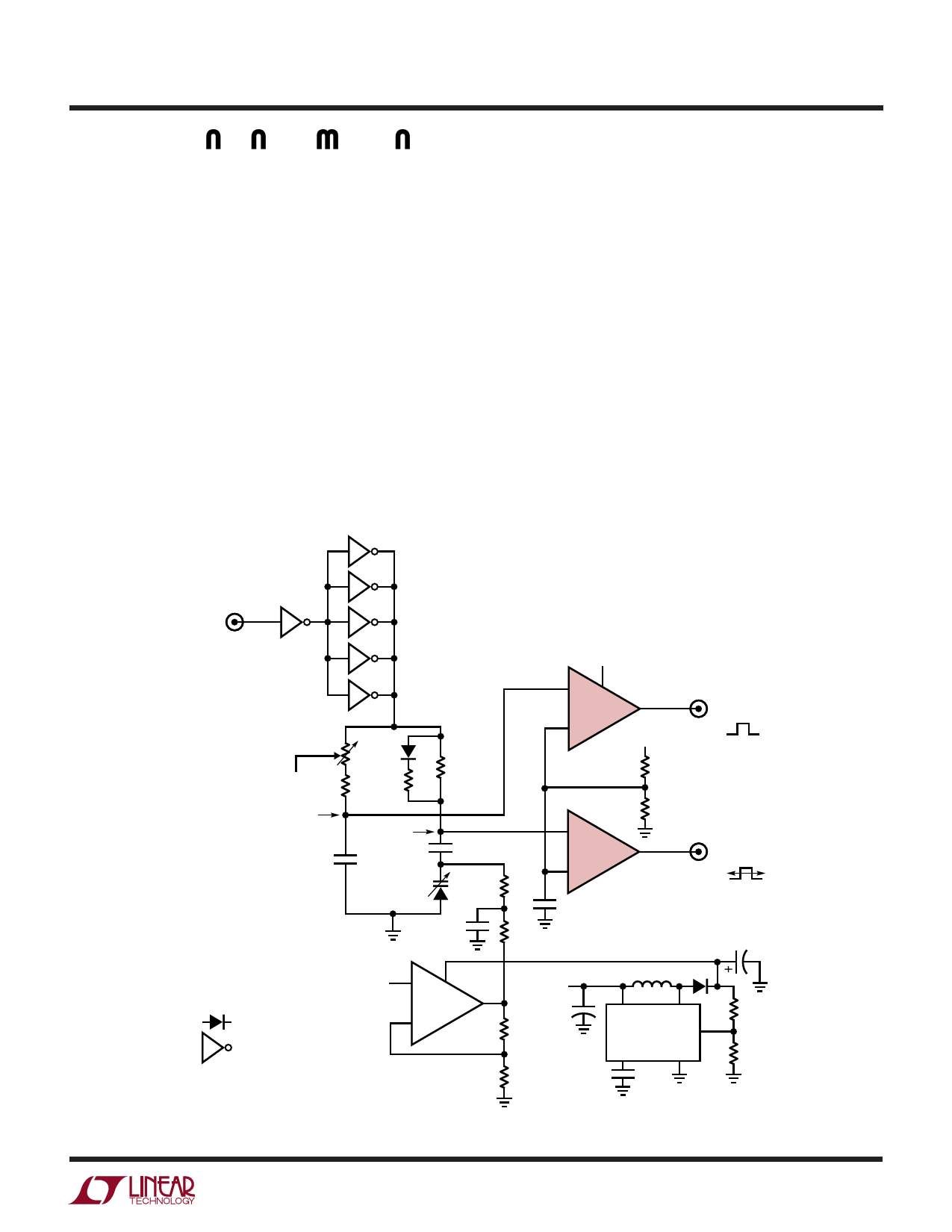
Voltage-Controlled Clock Skew Generator
It is sometimes necessary to generate pairs of identical
clock signals that are phase skewed in time. Further, it is
desirable to be able to set the amount of time skew via a
tuning voltage. Figure 18’s circuit does this by utilizing
the LT1720 to digitize phase information from a varactor-
tuned time domain bridge. A 0V to 2V control signal
provides ≈ ±10ns of output skew. This circuit operates
from a 2.7V to 6V supply.
CLOCK
INPUT
VCC
2.7V TO 6V
10ns
TRIM
“FIXED”
2k
2.5k*
2k*
14k
“SKEWED”
12pF†
MV-209
VARACTOR
DIODE
36pF†
0.005µF
= 1N4148
= 74HC04
* 1% FILM RESISTOR
** SUMIDA CD43-100
† POLYSTYRENE, 5%
INPUT
0V TO 2V ≈
±10ns
SKEW
+
A1
LT1077
–
+
C1
1/2 LT1720
–
VCC
2.5k
Q
FIXED
OUTPUT
2.5k
+
C2
1/2 LT1720
–
1M
0.1µF
Q′
SKEWED
OUTPUT
1M
47µF
VCC
+
2.2µF
6.2M*
1.82M*
L1**
VIN
SW
LT1317 FB
VC
GND
200pF
1.1M
100k
1720/21 F18
Figure 18. Voltage-Controlled Clock Skew
21
Share Link: 