74ALVC162334ADGG Ver la hoja de datos (PDF) - Philips Electronics
Número de pieza
componentes Descripción
Fabricante
74ALVC162334ADGG
Philips Electronics
74ALVC162334ADGG Datasheet PDF : 10 Pages
| |||
Philips Semiconductors
16-bit registered driver with inverted register enable
and 30Ω termination resistors (3-State)
Product specification
74ALVC162334A
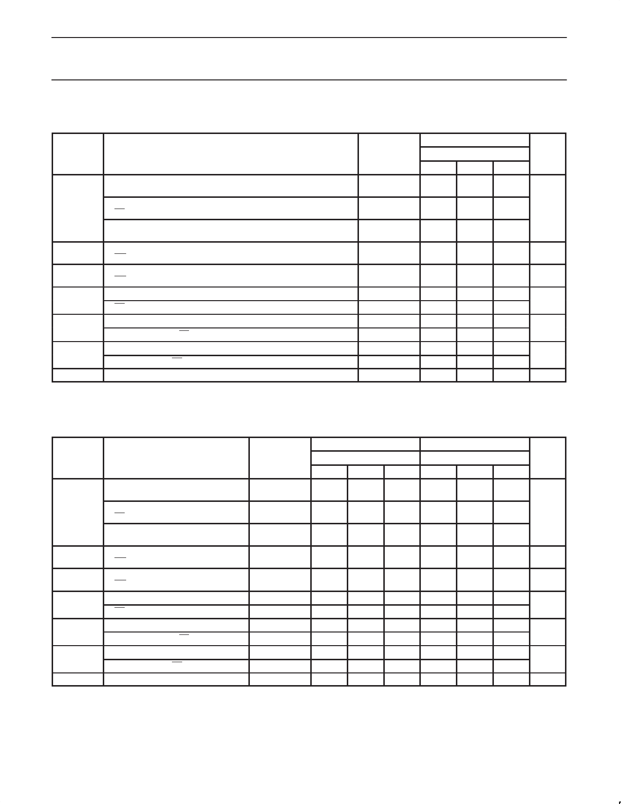
AC CHARACTERISTICS FOR VCC = 2.3 V TO 2.7 V RANGE
GND = 0 V; tr = tf ≤ 2.0 ns; CL = 30 pF
SYMBOL
PARAMETER
WAVEFORM
Propagation delay
An to Yn
1, 7
tPHL/tPLH
Propagation delay
LE to Yn
2, 7
Propagation delay
CP to Yn
4, 7
tPZH/tPZL
3-State output enable time
OE to Yn
6, 7
tPHZ/tPLZ
3-State output disable time
OE to Yn
6, 7
CP pulse width HIGH or LOW
4, 7
tW
LE pulse width HIGH
2, 7
Set-up time An to CP
5, 7
tSU
Set-up time An to LE
5, 7
Hold time An to CP
3, 7
th
Hold time An to LE
3, 7
fmax
Maximum clock pulse frequency
4, 7
NOTE:
1. All typical values are at VCC = 2.5 V and Tamb = 25°C.
AC CHARACTERISTICS FOR VCC = 3.0 V TO 3.6 V RANGE AND VCC = 2.7 V
GND = 0 V; tr = tf ≤ 2.5 ns; CL = 50 pF
LIMITS
SYMBOL
PARAMETER
WAVEFORM
VCC = 3.3 ± 0.3 V
MIN TYP1, 2 MAX
Propagation delay
An to Yn
1, 7
1.0
2.8
4.3
tPHL/tPLH
Propagation delay
LE to Yn
2, 7
1.3
2.8
4.4
Propagation delay
CP to Yn
4, 7
1.4
3.2
4.9
tPZH/tPZL
3-State output enable time
OE to Yn
6, 7
1.1
2.4
4.5
tPHZ/tPLZ
3-State output disable time
OE to Yn
6, 7
1.3
2.4
4.8
CP pulse width HIGH or LOW
tW
LE pulse width HIGH
4, 7
3.3
0.7
–
2, 7
3.3
0.6
–
Set-up time An to CP
tSU
Set-up time An to LE
5, 7
1.4
0.1
–
5, 7
1.5
0.2
–
Hold time An to CP
th
Hold time An to LE
3, 7
0.9
0.3
–
3, 7
1.4
0.3
–
fmax
Maximum clock pulse frequency
NOTES:
1. All typical values are measured Tamb = 25°C.
2. Typical value is measured at VCC = 3.3 V.
4, 7
150
240
–
LIMITS
VCC = 2.3 to 2.7 V
MIN TYP1 MAX
1.0
3.5
5.0
1.3
3.5
5.0
1.4
3.7
5.4
1.4
3.5
5.0
1.0
2.8
4.5
3.3
1.0
–
3.3
0.7
–
2.2
0.2
–
0.6
–0.1
–
0.4
0.4
–
1.4
0.4
–
150
190
–
LIMITS
VCC = 2.7 V
MIN TYP1 MAX
1.0
3.3
4.6
1.3
3.4
4.8
1.4
3.8
6.2
1.1
3.7
6.0
1.3
3.5
4.9
3.3
1.2
–
3.3
0.6
–
1.4
0.2
–
1.5
0.2
–
0.6
0.3
–
1.7
0.4
–
150
190
–
UNIT
ns
ns
ns
ns
ns
ns
MHz
UNIT
ns
ns
ns
ns
ns
ns
MHz
2000 Mar 14
6
Share Link: 