IDT70261L(2000) Ver la hoja de datos (PDF) - Integrated Device Technology
Número de pieza
componentes Descripción
Fabricante
IDT70261L
(Rev.:2000)
(Rev.:2000)
Integrated Device Technology
IDT70261L Datasheet PDF : 19 Pages
| |||
IDT70261S/L
High-Speed 16K x 16 Dual-Port Static RAM with Interrupt
Industrial and Commercial Temperature Ranges
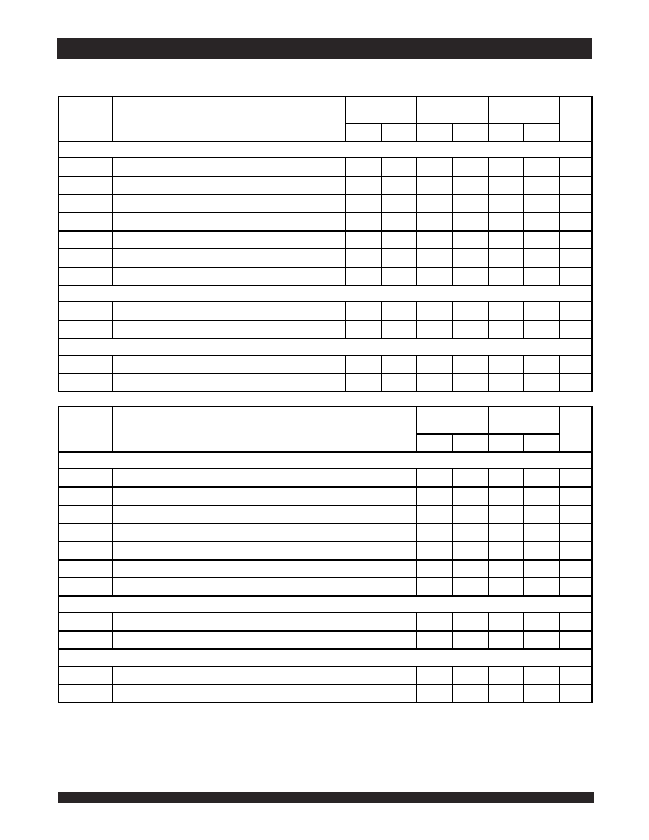
AC Electrical Characteristics Over the
Operating Temperature and Supply Voltage Range(6,7)
70261X15
Com'l Only
70261X20
Com'l & Ind
70261X25
Com'l & Ind
Symbol
BUSY TIMING (M/S=VIH)
Parameter
Min. Max. Min. Max. Min. Max. Unit
tBAA
BUSY Access Time from Address Match
tBDA
BUSY Disable Time from Address Not Matched
tBAC
BUSY Acce ss Time from Chip Enable Low
____
15
____
20
____
20
ns
____
15
____
20
____
20
ns
____
15
____
20
____
20
ns
tBDC
BUSY Acce ss Time from Chip Enable High
tAPS
Arbitration Priority Set-up Time(2)
____
15
____
17
____
17
ns
5
____
5
____
5
____
ns
tBDD
BUSY Disable to Valid Data(3)
tWH
Write Hold After BUSY(5)
BUSY TIMING (M/S=VIL)
tWB
BUSY Input to Write(4)
tWH
Write Hold After BUSY(5)
____
18
____
30
____
30
ns
12
____
15
____
17
____
ns
0
____
12
____
0
____
15
____
0
____
ns
17
____
ns
PORT-TO-PORT DELAY TIMING
tWDD
Write Pulse to Data Delay(1)
tDDD
Write Data Valid to Read Data Delay (1)
____
30
____
45
____
50
ns
____
25
____
30
____
35
ns
3039 tbl 14a
70261X35
Com'l & Ind
70261X55
Com'l & Ind
Symbol
BUSY TIMING (M/S=VIH)
Parameter
Min. Max. Min. Max. Unit
tBAA
BUSY Access Time from Address Match
tBDA
BUSY Disable Time from Address Not Matched
tBAC
BUSY Acce ss Time from Chip Enable Low
____
20
____
45
ns
____
20
____
40
ns
____
20
____
40
ns
tBDC
BUSY Acce ss Time from Chip Enable High
tAPS
Arbitration Priority Set-up Time(2)
____
20
____
35
ns
5
____
5
____
ns
tBDD
BUSY Disable to Valid Data(3)
tWH
Write Hold After BUSY(5)
BUSY TIMING (M/S=VIL)
tWB
BUSY Input to Write(4)
tWH
Write Hold After BUSY(5)
____
35
____
40
ns
25
____
25
____
ns
0
____
0
____
ns
25
____
25
____
ns
PORT-TO-PORT DELAY TIMING
tWDD
Write Pulse to Data Delay(1)
____
60
____
80
ns
tDDD
Write Data Valid to Read Data Delay (1)
____
45
____
65
ns
NOTES:
3039 tbl 14b
1. Port-to-port delay through RAM cells from writing port to reading port, refer to "Timing Wave form of Write with Port-to-Port Read and BUSY (M/S = VIH)".
2. To ensure that the earlier of the two ports wins.
3. tBDD is a calculated parameter and is the greater of 0, tWDD – tWP (actual), or tDDD – tDW (actual).
4. To ensure that the write cycle is inhibited on port "B" during contention on port "A".
5. To ensure that a write cycle is completed on port "B" after contention on port "A".
6. 'X' in part numbers indicates power rating (S or L).
61.412
Share Link: 