IH6108CJE Ver la hoja de datos (PDF) - Intersil
Número de pieza
componentes Descripción
Fabricante
IH6108CJE Datasheet PDF : 9 Pages
| |||
IH6108
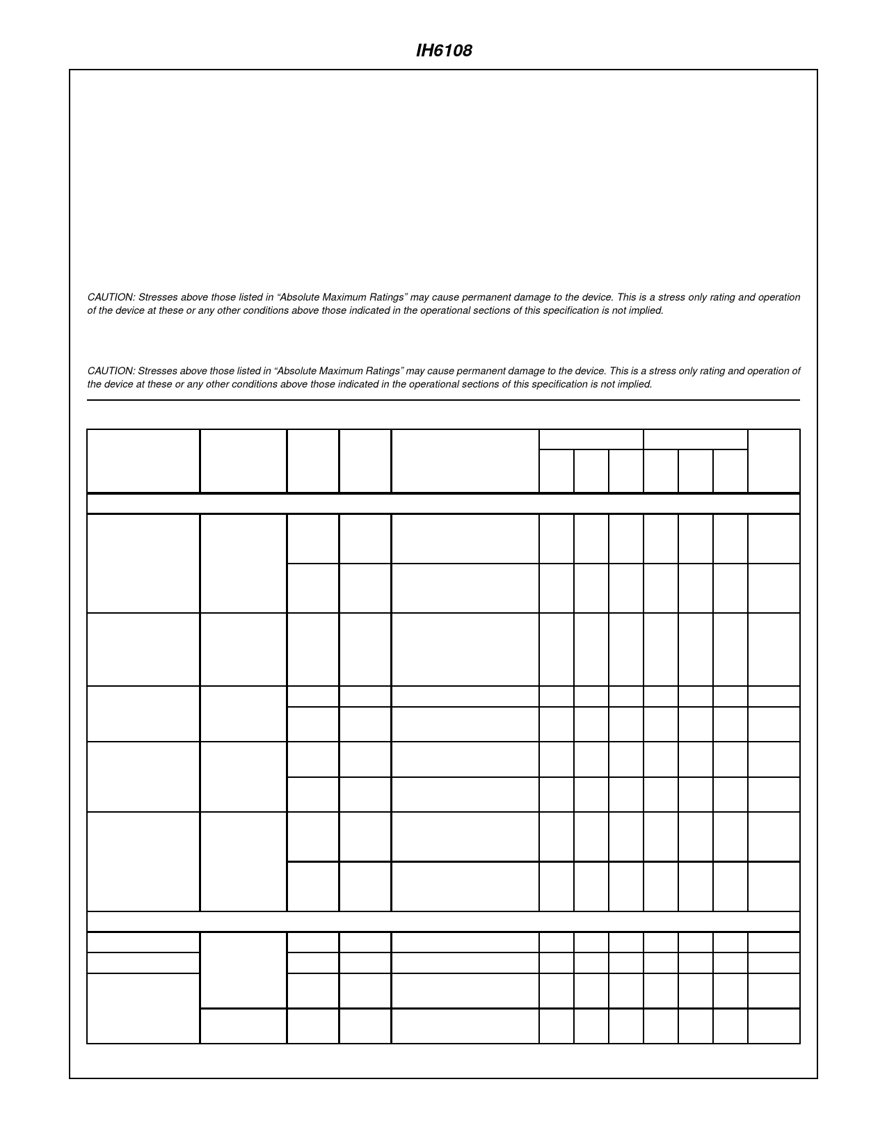
Absolute Maximum Ratings
VIN (A, EN) to Ground . . . . . . . . . . . . . . . . . . . . . . . . . . -15V to 15V
VS or VD to V+ . . . . . . . . . . . . . . . . . . . . . . . . . . . . . . . . . . .0V, -36V
VS to VD to V- . . . . . . . . . . . . . . . . . . . . . . . . . . . . . . . . . . . . 0V, 36V
V+ to Ground . . . . . . . . . . . . . . . . . . . . . . . . . . . . . . . . . . . . . . . 18V
V- to Ground . . . . . . . . . . . . . . . . . . . . . . . . . . . . . . . . . . . . . . . .-18V
Current (Any Terminal) . . . . . . . . . . . . . . . . . . . . . . . . . . . . . . 30mA
Current (Analog Source or Drain) . . . . . . . . . . . . . . . . . . . . . . 20mA
Thermal Information
Thermal Resistance (Typical, Note 1)
θJA (oC/W) θJC (oC/W)
PDIP Package . . . . . . . . . . . . . . . . . . . 100
N/A
CERDIP Package . . . . . . . . . . . . . . . .
75
20
Maximum Junction Temperature (Hermetic Package) . . . . . . . . 175oC
Maximum Junction Temperature (Plastic Package) . . . . . . . . 150oC
Maximum Storage Temperature Range . . . . . . . . . .-65oC to 150oC
Maximum Lead Temperature (Soldering 10s) . . . . . . . . . . . . . 300oC
Operating Conditions
Temperature Range
C Suffix . . . . . . . . . . . . . . . . . . . . . . . . . . . . . . . . . . . .0oC to 70oC
M Suffix . . . . . . . . . . . . . . . . . . . . . . . . . . . . . . . . . -55oC to 125oC
CAUTION: Stresses above those listed in “Absolute Maximum Ratings” may cause permanent damage to the device. This is a stress only rating and operation
of the device at these or any other conditions above those indicated in the operational sections of this specification is not implied.
NOTE:
1. θJA is measured with the component mounted on an evaluation PC board in free air.
CAUTION: Stresses above those listed in “Absolute Maximum Ratings” may cause permanent damage to the device. This is a stress only rating and operation of
the device at these or any other conditions above those indicated in the operational sections of this specification is not implied.
Electrical Specifications V+ = 15V, V- = -15V, VEN = +5V, Ground = 0V, Unless Otherwise Specified, (Note 4)
NO
M SUFFIX (oC) C SUFFIX (oC)
TESTS
PARAMETER
MEASURED PER TYP
TERMINAL TEMP 25oC
TEST CONDITIONS
-55 25 125 0 25 70
UNITS
SWITCH
rDS(ON)
∆rDS(ON)
IS(OFF)
ID(OFF)
ID(ON)
INPUT
S to D
S
D
D
8
180 VD = +10V, IS = -1.0mA
300 300 400 350 350 450
Ω
Sequence Each Switch On
VAL = 0.8V, VAH = 2.4V
8
150 VD = -10V, IS = -1.0mA
300 300 400 350 350 450
Ω
Sequence Each Switch On
VAL = 0.8V, VAH = 2.4V
20 ∆rDS(ON) =
-
-
-
-
-
-
%
-r--D-----S-----(--O-----N--r---D)--M---S---A-(--O-X-----N–---r-)--D-A----SV----(G--O-˙-----N----)---M-----I--N--- ,
VS = ±10V
8
0.002 VS = 10V, VD = -10V
- ±0.5 ±50 - ±1 ±50 nA
8
0.002 VS = -10V, VD = 10V,
VEN = 0.8V
- ±0.5 ±50 - ±1 ±50 nA
1
0.03 VD = 10V, VS = -10V,
VEN = 0.8V
- ±2 ±100 - ±5 ±100 nA
1
0.03 VD = -10V, VS = 10V,
VEN = 0.8V
- ±2 ±100 - ±5 ±100 nA
8
0.1 VS(ALL) = VD = 10V,
- ±2 ±100 - ±5 ±100 nA
Sequence Each Switch On
VAL = 0.8V, VAH = 2.4V
8
0.1 VS(ALL) = VD = -10V,
- ±2 ±100 - ±5 ±100 nA
Sequence Each Switch On
VAL = 0.8V, VAH = 2.4V
IAN(ON) or IA(on)
A0, A1, or A2
3
IAN(OFF) IA(off)
IA
Inputs
3
A0, A1, A2
3
0.01 VA = 0V
0.01 VA = 14V
0.01 VEN = 5V, All VA = 0V
(Address Pins)
- -10 -30 - -10 -30 µA
- 10 30 - 10 30
µA
- -10 -30 - -10 -30 µA
EN
1
0.01 VEN = 0V, All VA = 0V
- -10 -30 - -10 -30 µA
(Address Pins)
12-129
Share Link: 