NTE1508 Ver la hoja de datos (PDF) - NTE Electronics
Número de pieza
componentes Descripción
Fabricante
NTE1508 Datasheet PDF : 3 Pages
| |||
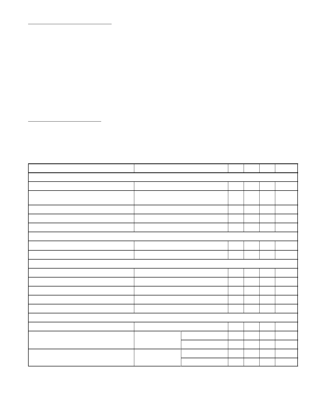
Absolute Maximum Ratings:
Power Dissipation (Note 1) . . . . . . . . . . . . . . . . . . . . . . . . . . . . . . . . . . . . . . . . . . . . . . . . . . . . . 1365mW
Supply Voltage . . . . . . . . . . . . . . . . . . . . . . . . . . . . . . . . . . . . . . . . . . . . . . . . . . . . . . . . . . . . . . . . . . . . 25V
Voltage on Output Drivers . . . . . . . . . . . . . . . . . . . . . . . . . . . . . . . . . . . . . . . . . . . . . . . . . . . . . . . . . . 25V
Input Signal Overvoltage (Note 2) . . . . . . . . . . . . . . . . . . . . . . . . . . . . . . . . . . . . . . . . . . . . . . . . . . . ±35V
Divider Voltage . . . . . . . . . . . . . . . . . . . . . . . . . . . . . . . . . . . . . . . . . . . . . . . . . . . . . . . . . . . –100mV to V+
Reference Load Current . . . . . . . . . . . . . . . . . . . . . . . . . . . . . . . . . . . . . . . . . . . . . . . . . . . . . . . . . . 10mA
Storage Temperature Range . . . . . . . . . . . . . . . . . . . . . . . . . . . . . . . . . . . . . . . . . . . . . . –55° to +150°C
Lead Temperature (During soldering, 10sec) . . . . . . . . . . . . . . . . . . . . . . . . . . . . . . . . . . . . . . . +260°C
Note 1. The maximum junction temperature of the NTE1508 is +100°C. Device must be derated for
operation at elevated temperatures. Junction to ambient thermal resistance is 55°C/W.
Note 2. Pin5 input current must be limited to ±3mA. The addition of a 39kΩ resistor in series with
Pin5 allows ±100V signals without damage.
Electrical Characteristics:
(Note 2, unless otherwise specified, all specifications apply with the
following conditions:
3VDC ≤ V+ ≤ 20VDC
3VDC ≤ VLED ≤ V+
–0.015V ≤ VRLO ≤ 12VDC
–0.015V ≤ VRHI ≤ 12VDC
VREF, VRHI, VRLO ≤ (V+ –1.5V)
0V ≤ VIN ≤ V+ –1.5V
TA +25°C, IL(REF) = 0.2mA,
VLED = 3V, Pin9 connected to Pin3
(Bar Mode)
Parameter
Test Conditions
Min Typ Max Unit
Comparator
Offset Voltage, Buffer, and First Comparator
Offset Voltage, Buffer, and Any Other
Comparator
0V ≤ VRLO = VRHI ≤ 12V, ILED = 1mA
0V ≤ VRLO = VRHI ≤ 12V, ILED = 1mA
– 3 10 mV
– 3 15 mV
Gain (∆ILED/∆VIN)
Input Bias Current (At Pin5)
Input Signal Overdrive
IL(REF) = 2mA, ILED = 10mA
0V ≤ VIN ≤ V+ =1.5V
No Change is Display
3 8 – mA/mV
– 25 100 nA
–35 – +35 V
Voltage Divider
Divider Resistance
Total, Pin6 to Pin4
8 12 17 kΩ
Accuracy
Note 3
– 0.5 2.0 %
Voltage Reference
Output Voltage
Line Regulation
0.1mA ≤ IL(REF) ≤ 4mA, V+ = VLED = 5V 1.2 1.28 1.34
V
3V ≤ V+ ≤ 18V
– 0.01 0.03 %/V
Load Regulation
Output Voltage Change with Temperature
Adjust Pin Current
0.1mA ≤ IL(REF) ≤ 4mA, V+ = VLED = 5V – 0.4 2.0
%
0° ≤ TA ≤ +70°C, IL(REF) = 1mA, V+ = 5V –
1
–
%
– 75 120 µA
Output Drivers
LED Current
LED Current Difference (Between Largest and
Smallest LED Currents)
LED Current Regulation
V+ = VLED = 5V, IL(REF) = 1mA
VLED = 5V
ILED = 2mA
ILED = 20mA
2V ≤ VLED ≤ 17V ILED = 2mA
ILED = 20mA
7 10 13 mA
– 0.12 0.4 mA
– 1.2 3.0 mA
– 0.1 0.25 mA
–13
mA
Note 3. Accuracy is measured referred to +10.000VDC at Pin6, with 0.000VDC at Pin4. At lower full–
scale voltages, buffer and comparator offset voltage may add significant error.
Share Link: 