MKL33Z128VLH4 Ver la hoja de datos (PDF) - Freescale Semiconductor
Número de pieza
componentes Descripción
Fabricante
MKL33Z128VLH4
Freescale Semiconductor
MKL33Z128VLH4 Datasheet PDF : 63 Pages
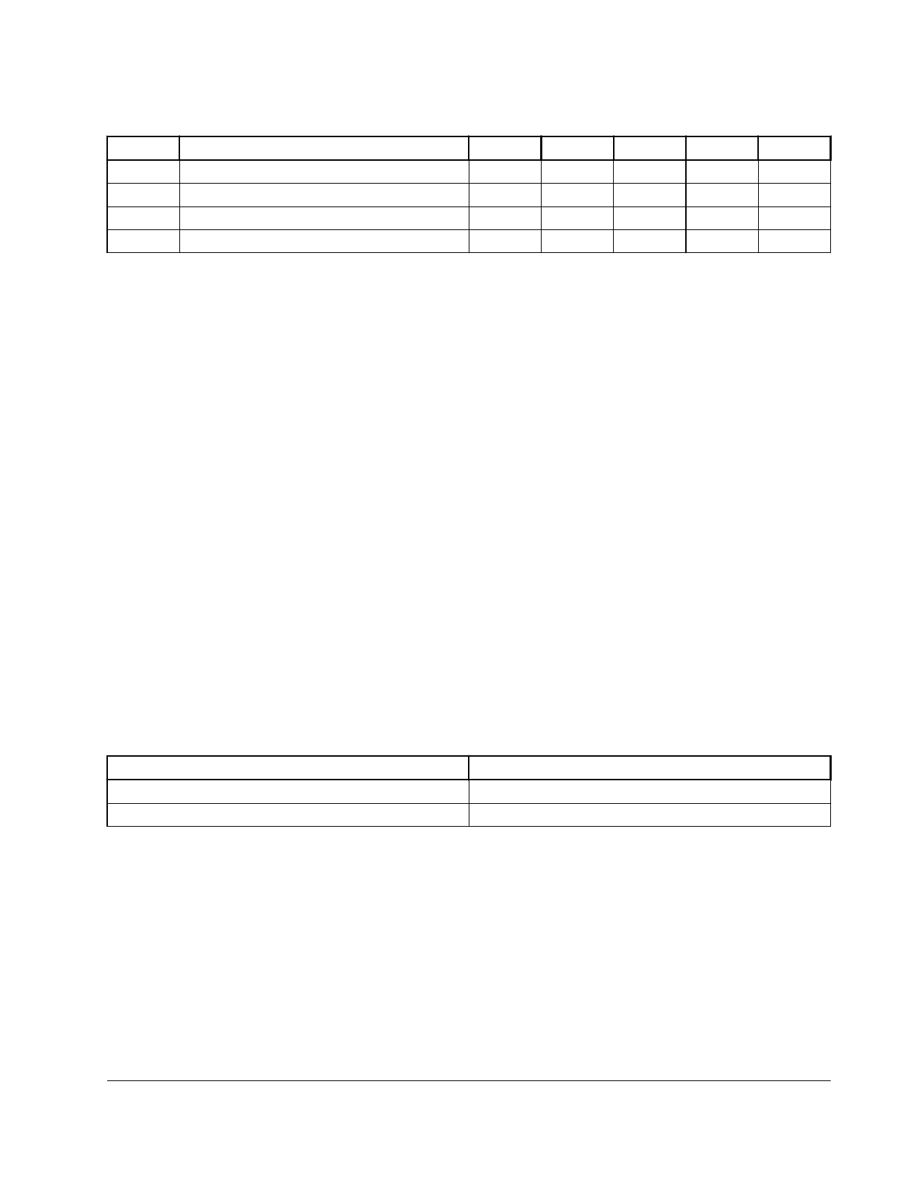
| |||
Dimensions
Symbol Description
VLL3 VLL3 voltage
VLL1 VLL1 voltage
VLL2 VLL2 voltage
VLL3 VLL3 voltage
Table 42. LCD electricals (continued)
Min.
—
—
—
—
Typ.
—
—
—
—
Max.
3 x VIREG
VDDA / 3
VDDA / 1.5
VDDA
Unit
V
V
V
V
Notes
4
5
5
5
1. The actual value used could vary with tolerance.
2. For highest glass capacitance values, LCD_GCR[LADJ] should be configured as specified in the LCD Controller
chapter within the device's reference manual.
3. VIREG maximum should never be externally driven to any level other than VDD - 0.15 V
4. VLL1, VLL2 and VLL3 are a function of VIREG only when the regulator is enabled (GCR[RVEN]=1) and the charge
pump is enabled (GCR[CPSEL]=1).
5. VLL1, VLL2 and VLL3 are a function of VDDA only under either of the following conditions:
• The charge pump is enabled (GCR[CPSEL]=1), the regulator is disabled (GCR[RVEN]=0), and VLL3 = VDDA
through the internal power switch (GCR[VSUPPLY]=0).
• The resistor bias string is enabled (GCR[CPSEL]=0), the regulator is disabled (GCR[RVEN]=0), and VLL3 is
connected to VDDA externally (GCR[VSUPPLY]=1).
4 Dimensions
4.1 Obtaining package dimensions
Package dimensions are provided in package drawings.
To find a package drawing, go to freescale.com and perform a keyword search for the
drawing’s document number:
If you want the drawing for this package
64-pin LQFP
64-pin MAPBGA
Then use this document number
98ASS23234W
98ASA00420D
Kinetis KL33 With Up To 256 KB Flash, Rev3, 08/2014.
51
Freescale Semiconductor, Inc.
Share Link: 