HEF4543BP Ver la hoja de datos (PDF) - NXP Semiconductors.
Número de pieza
componentes Descripción
Fabricante
HEF4543BP Datasheet PDF : 16 Pages
| |||
NXP Semiconductors
HEF4543B
BCD to 7-segment latch/decoder/driver
VI
LE input
VSS
VM
tW
VI
D2 input
VM
VSS
VOH
tsu
th
Qg output
VOL
001aaj799
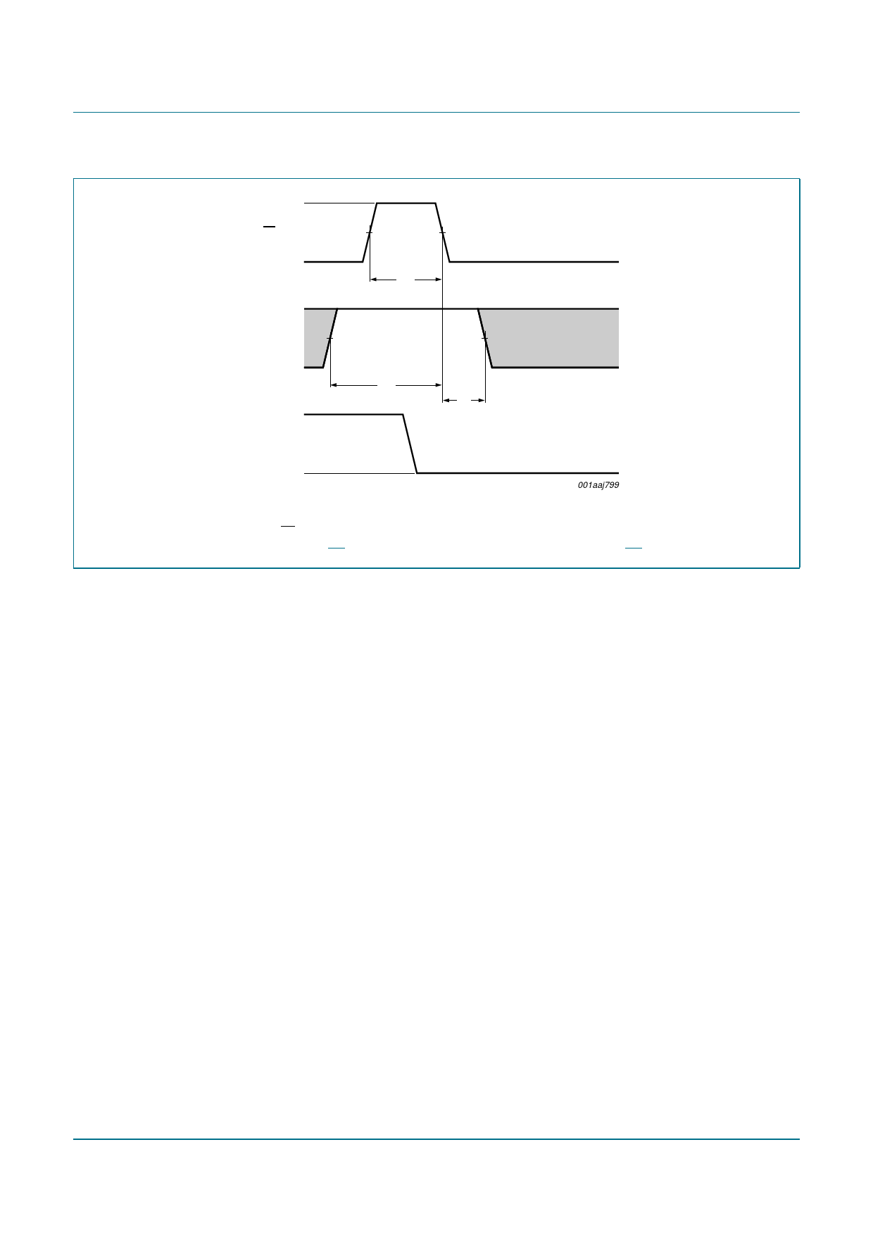
Fig 6.
Conditions:
D3 = BL = LOW; D0 = D1 = LE = HIGH
Waveforms showing minimum LE pulse width, set-up, and hold time for DC to LE
HEF4543B_5
Product data sheet
Rev. 05 — 27 October 2009
© NXP B.V. 2009. All rights reserved.
9 of 16
Share Link: 