MC14069UB Ver la hoja de datos (PDF) - Motorola => Freescale
Número de pieza
componentes Descripción
Fabricante
MC14069UB Datasheet PDF : 4 Pages
| |||
MOTOROLA
SEMICONDUCTOR TECHNICAL DATA
MC14068B
See Page 6-5
Hex Inverter
The MC14069UB hex inverter is constructed with MOS P–channel and
N–channel enhancement mode devices in a single monolithic structure.
These inverters find primary use where low power dissipation and/or high
noise immunity is desired. Each of the six inverters is a single stage to
minimize propagation delays.
• Supply Voltage Range = 3.0 Vdc to 18 Vdc
• Capable of Driving Two Low–Power TTL Loads or One Low–Power
Schottky TTL Load Over the Rated Temperature Range
• Triple Diode Protection on All Inputs (see Page 5–2)
• Pin–for–Pin Replacement for CD4069UB
ÎÎÎÎÎÎÎÎÎÎÎÎÎÎÎÎÎÎÎÎÎ • Meets JEDEC UB Specifications
ÎÎÎÎÎÎÎÎÎÎÎÎÎÎÎÎÎÎÎÎÎÎÎÎÎÎÎÎÎÎÎÎÎÎÎÎÎÎÎÎÎÎ MAXIMUM RATINGS* (Voltages Referenced to VSS)
Symbol
Parameter
Value
Unit
ÎÎÎÎÎÎÎÎÎÎÎÎÎÎÎÎÎÎÎÎÎ VDD DC Supply Voltage
– 0.5 to + 18.0
V
ÎÎÎÎÎÎÎÎÎÎÎÎÎÎÎÎÎÎÎÎÎ Vin, Vout Input or Output Voltage (DC or Transient) – 0.5 to VDD + 0.5 V
ÎÎÎÎÎÎÎÎÎÎÎÎÎÎÎÎÎÎÎÎÎ Iin, Iout Input or Output Current (DC or Transient),
± 10
mA
ÎÎÎÎÎÎÎÎÎÎÎÎÎÎÎÎÎÎÎÎÎ per Pin
ÎÎÎÎÎÎÎÎÎÎÎÎÎÎÎÎÎÎÎÎÎ PD Power Dissipation, per Package†
ÎÎÎÎÎÎÎÎÎÎÎÎÎÎÎÎÎÎÎÎÎ Tstg Storage Temperature
ÎÎÎÎÎÎÎÎÎÎÎÎÎÎÎÎÎÎÎÎÎÎÎÎÎÎÎÎÎÎÎÎÎÎÎÎÎÎÎÎÎÎ TL
Lead Temperature (8–Second Soldering)
500
mW
– 65 to + 150
_C
260
_C
* Maximum Ratings are those values beyond which damage to the device may occur.
†Temperature Derating:
Plastic “P and D/DW” Packages: – 7.0 mW/_C From 65_C To 125_C
Ceramic “L” Packages: – 12 mW/_C From 100_C To 125_C
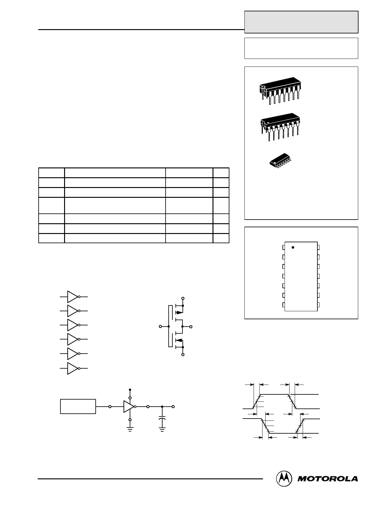
LOGIC DIAGRAM
1
2
3
4
VDD = PIN 14
VSS = PIN 7
5
6
CIRCUIT SCHEMATIC
(1/6 OF CIRCUIT SHOWN)
VDD
INPUT*
OUTPUT
9
8
MC14069UB
L SUFFIX
CERAMIC
CASE 632
P SUFFIX
PLASTIC
CASE 646
D SUFFIX
SOIC
CASE 751A
ORDERING INFORMATION
MC14XXXUBCP
MC14XXXUBCL
MC14XXXUBD
Plastic
Ceramic
SOIC
TA = – 55° to 125°C for all packages.
PIN ASSIGNMENT
IN 1 1
OUT 1 2
IN 2 3
OUT 2 4
IN 3 5
OUT 3 6
VSS 7
14 VDD
13 IN 6
12 OUT 6
11 IN 5
10 OUT 5
9 IN 4
8 OUT 4
11
10
13
12
VSS
* Double diode protection on all
inputs not shown.
PULSE
GENERATOR
VDD
14
OUTPUT
INPUT
7 VSS
CL
20 ns
INPUT
tPHL
OUTPUT
90%
50%
10%
90%
50%
10%
tTHL
Figure 1. Switching Time Test Circuit and Waveforms
REV 3
1/94
©MMOotoTrOolaR, IOncL. A199C5MOS LOGIC DATA
20 ns
VDD
VSS
tPLH
VOH
VOL
tTLH
MC14069UB
1
Share Link: 