LD7750A Ver la hoja de datos (PDF) - Unspecified
Número de pieza
componentes Descripción
Fabricante
LD7750A Datasheet PDF : 19 Pages
| |||
LD7750A
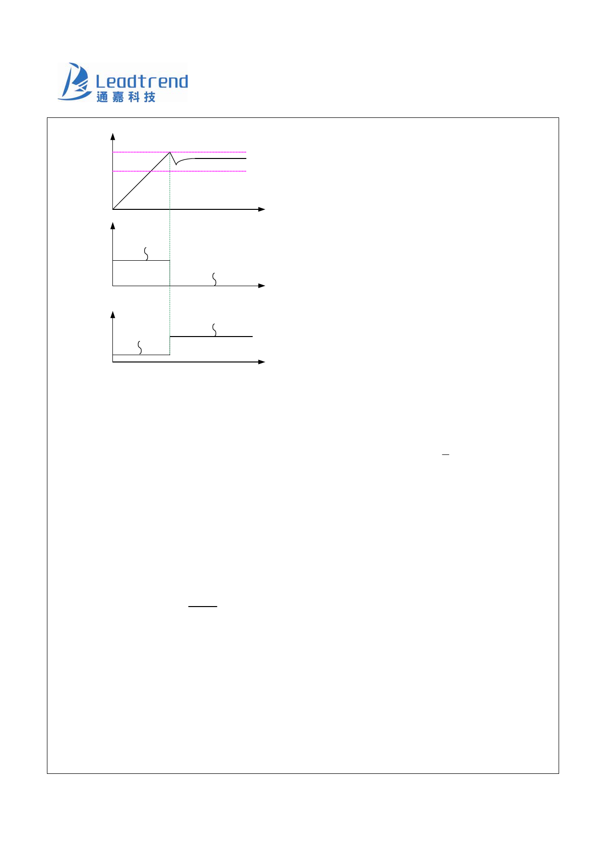
Vcc
UVLO(on)
UVLO(off)
Nevertheless, it is strongly recommended to add a small
R-C filter (as shown in Fig. 16) for higher power
applications to avoid the CS pin being damaged by the
negative turn-on spike.
t
HV Current
1mA
Vcc current
Startup Current
~ 0mA (off)
t
Operating Current
(Supply from Auxiliary Winding)
Fig. 14
Current Sensing, Leading-edge Blanking
and the Negative Spike on CS Pin
The typical current mode PWM controller feeds back both
current signal and voltage signal to close the control loop
and achieve regulation. The LD7750A detects the primary
MOSFET current from the CS pin, which is not only for the
peak current mode control but also for the pulse-by-pulse
current limit. The maximum voltage threshold of the
current sensing pin is set as 0.85V. Thus the MOSFET
peak current can be calculated as:
IPEAK(MAX)
=
0.85V
RS
A 250nS leading-edge blanking (LEB) time is included in
the input of CS pin to prevent false-trigger caused by the
current spike. For those low power applications, if the total
pulse width of the turn-on spike is less than 250nS and
the negative spike on the CS pin is above -0.3V, the R-C
filter (as shown in Fig.15) is removable.
However, the total pulse width of the turn-on spike is
related to the output power, circuit design and PCB layout.
Output Stage and Maximum Duty-Cycle
An output stage of a CMOS buffer, with typical 500mA
driving capability, is incorporated to drive a power
MOSFET directly. And the maximum duty-cycle of
LD7750A is limited to 75% to avoid the transformer
saturation.
Voltage Feedback Loop
The voltage feedback signal is provided from the TL431 in
the secondary side through the photo-coupler to the
COMP pin of LD7750A. The input stage of LD7750A,
like the UC384X, is incorporated with 2 diodes voltage
offset circuit and a voltage divider with 1/3 ratio.
Therefore,
V+ (PWM COMPARATOR
)
=
1
3
× (VCOMP
−
2VF )
A pull-high resistor is embedded internally and thus no
external one is required for it.
Switching Frequency
The LD7750A is implemented with frequency swapping
function which helps the power supply designers both
optimize EMI performance and lower system cost. The
switching frequency substantially centers at 65KHz, and
trembles within the range of ±4KHz.
Leadtrend Technology Corporation
LD7750A-DS-00 June 2010
10
www.leadtrend.com.tw
Share Link: 