LTC2633AHTS8-HZ8 Ver la hoja de datos (PDF) - Linear Technology
NГғmero de pieza
componentes DescripciГіn
Fabricante
LTC2633AHTS8-HZ8 Datasheet PDF : 24 Pages
| |||
LTC2633
Operation
The format of the three data bytes is shown in Figure
3. The first byte of the input word consists of the 4-bit
command, followed by the 4-bit DAC address. The next
two bytes contain the 16-bit data word, which consists
of the 12-, 10- or 8-bit input code, MSB to LSB, followed
by 4, 6 or 8 don’t-care bits (LTC2633-12, LTC2633-10
and LTC2633-8 respectively). A typical LTC2633 write
transaction is shown in Figure 4.
The command bit assignments (C3-C0) and address (A3-
A0) assignments are shown in Tables 3 and 4. The first
four commands in the table consist of write and update
operations. A write operation loads a 16-bit data word
from the 32-bit shift register into the input register. In an
update operation, the data word is copied from the input
register to the DAC register. Once copied into the DAC
register, the data word becomes the active 12-, 10-, or
8-bit input code, and is converted to an analog voltage at
the DAC output. Write to and update combines the first
two commands. The update operation also powers up the
DAC if it had been in power-down mode. The data path
and registers are shown in the Block Diagram.
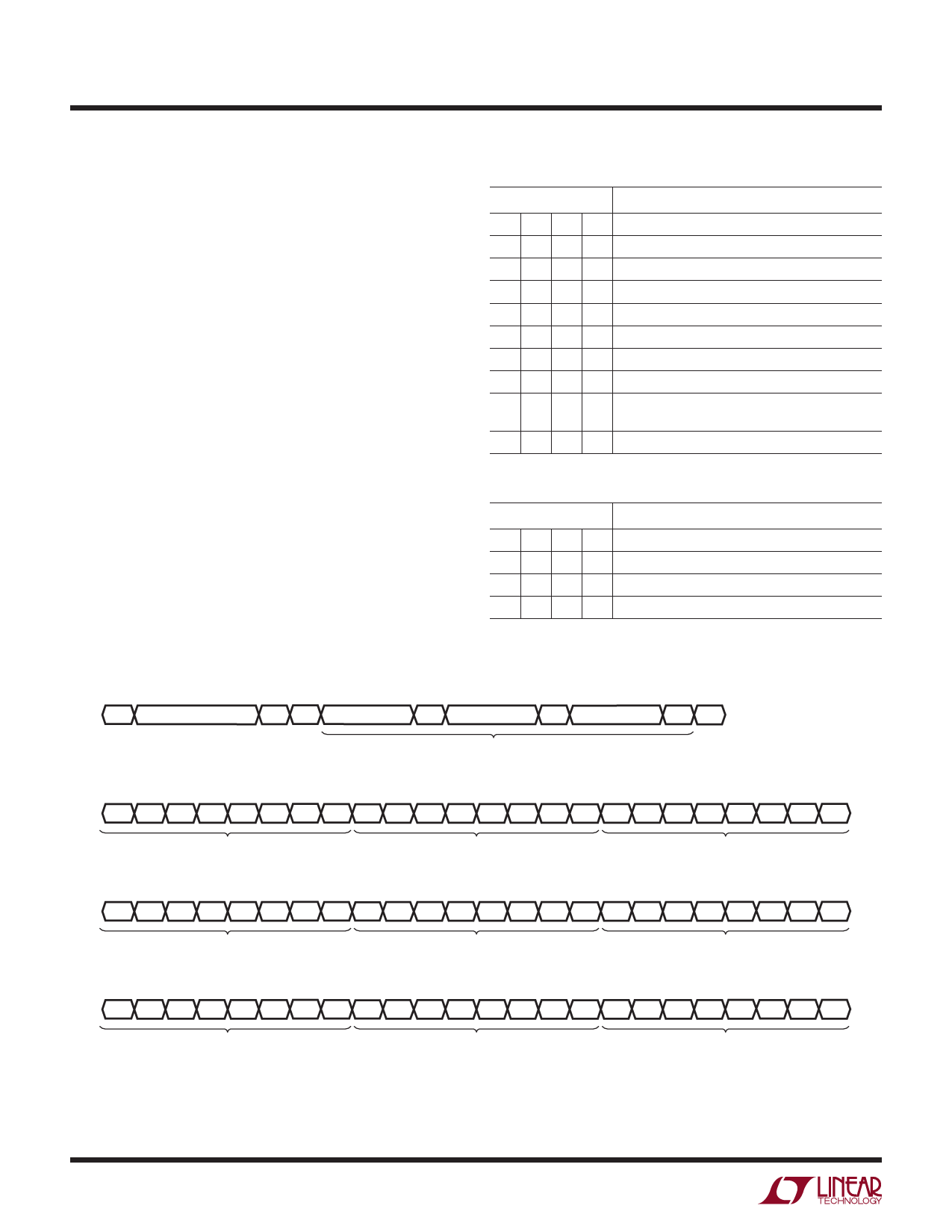
Table 3. Command Codes
COMMAND*
C3 C2 C1 C0
0 0 0 0 Write to Input Register n
0 0 0 1 Update (Power-Up) DAC Register n
0 0 1 0 Write to Input Register n, Update (Power-Up) All
0 0 1 1 Write to and Update (Power-Up) DAC Register n
0 1 0 0 Power-Down n
0 1 0 1 Power-Down Chip (All DAC’s and Reference)
0 1 1 0 Select Internal Reference (Power-Up Reference)
0 1 1 1 Select External Reference (Power-Down Internal
Reference)
1 1 1 1 No Operation
*Command codes not shown are reserved and should not be used.
Table 4. Address Codes
ADDRESS (n)*
A3 A2 A1 A0
0 0 0 0 DAC A
0 0 0 1 DAC B
1 1 1 1 All DACs
* Address codes not shown are reserved and should not be used.
WRITE WORD PROTOCOL LTC2633
S
SLAVE ADDRESS
W A 1ST DATA BYTE A 2ND DATA BYTE A 3RD DATA BYTE A P
INPUT WORD
INPUT WORD (LTC2633-12)
C3 C2 C1 C0 A3 A2 A1 A0 D11 D10 D9 D8 D7 D6 D5 D4 D3 D2 D1 D0 X X X X
1ST DATA BYTE
2ND DATA BYTE
3RD DATA BYTE
INPUT WORD (LTC2633-10)
C3 C2 C1 C0 A3 A2 A1 A0 D9 D8 D7 D6 D5 D4 D3 D2 D1 D0 X X X X X X
1ST DATA BYTE
2ND DATA BYTE
3RD DATA BYTE
INPUT WORD (LTC2633-8)
C3 C2 C1 C0 A3 A2 A1 A0 D7 D6 D5 D4 D3 D2 D1 D0 X X X X X X X X
1ST DATA BYTE
2ND DATA BYTE
3RD DATA BYTE
2633 F03
Figure 3. Command and Data Input Format
2633fb
18
Share Link: 