673M-01 Ver la hoja de datos (PDF) - Integrated Device Technology
Número de pieza
componentes Descripción
Fabricante
673M-01 Datasheet PDF : 9 Pages
| |||
ICS673-01
PLL BUILDING BLOCK
PLL BUILDING BLOCK
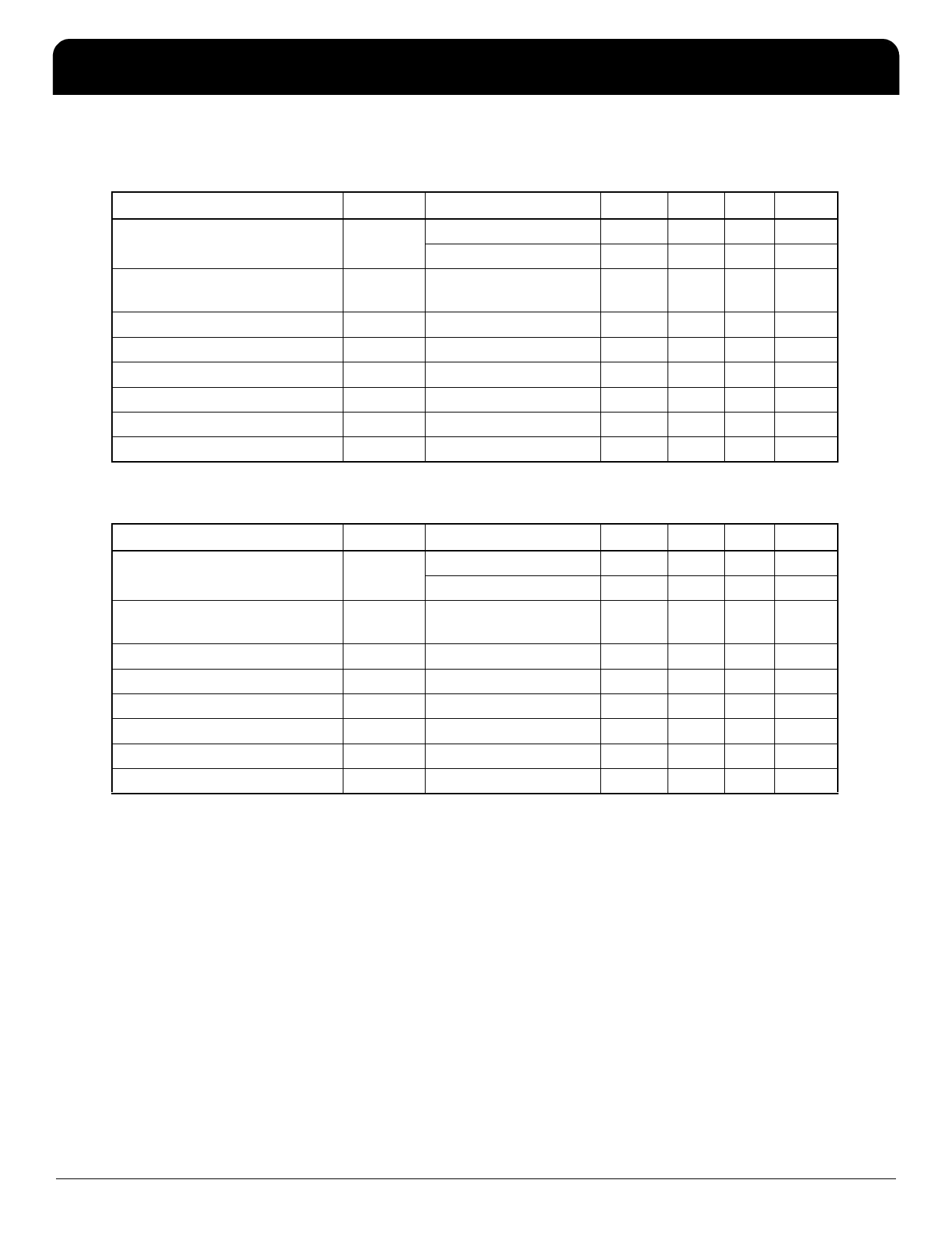
AC Electrical Characteristics
VDD = 3.3 V ±5%, Ambient Temperature -40 to +85° C, CLOAD at CLK = 15 pF, unless stated otherwise.
Parameter
Symbol
Conditions
Min. Typ. Max. Units
Output Clock Frequency
(from pin CLK)
fCLK SEL = 1
SEL = 0
1
100 MHz
0.25
25 MHz
Input Clock Frequency
fREF
(into pins REFIN or FBIN)
Note 1
8 MHz
Output Rise Time
Output Fall Time
Output Clock Duty Cycle
Jitter, Absolute peak-to-peak
VCO Gain
Charge Pump Current
tOR 0.8 to 2.0 V
tOF 2.0 to 0.8 V
tDC At VDD/2
tJ
KO
Icp
1.2 2
ns
0.75 1.5 ns
40
50 60
%
250
ps
190
MHz/V
2.5
µA
VDD = 5.0 V ±10%, Ambient Temperature -40 to +85° C, CLOAD at CLK = 15 pF, unless stated otherwise.
Parameter
Symbol
Conditions
Min. Typ. Max. Units
Output Clock Frequency
(from pin CLK)
fCLK SEL = 1
SEL = 0
1
120 MHz
0.25
30 MHz
Input Clock Frequency
fREF
(into pins REFIN or FBIN)
Note 1
8 MHz
Output Rise Time
Output Fall Time
Output Clock Duty Cycle
Jitter, Absolute peak-to-peak
VCO Gain
Charge Pump Current
tOR 0.8 to 2.0 V
tOF 2.0 to 0.8 V
tDC At VDD/2
tJ
KO
Icp
0.5 1
ns
0.5 1
ns
45
50 55
%
150
ps
190
MHz/V
2.4
µA
Note 1: Minimum input frequency is limited by loop filter design. 1 kHz is a practical minimum limit.
External Components
The ICS673-01 requires a minimum number of external
components for proper operation. A decoupling capacitor of
0.01µF should be connected between VDD and GND as
close to the ICS673-01 as possible. A series termination
resistor of 33Ω may be used at the clock output.
Special considerations must be made in choosing loop
components CS and CP. These can be found online at
http://www.icst.com/products/telecom/loopfiltercap.htm
Avoiding PLL Lockup
In some applications, the ICS673-01 can “lock up” at the
maximum VCO frequency. This is usually caused by power
supply glitches or a very slow power supply ramp. This
situation also occurs if the external divider starts to fail at
high input frequencies. The usual failure mode of a divider
circuit is that the output of the divider begins to miss clock
edges. The phase detector interprets this as a too low
output frequency and increases the VCO frequency. The
IDT™ / ICS™ PLL BUILDING BLOCK
4
ICS673-01 REV Q 071906
Share Link: 