SI3443DV(1997) Ver la hoja de datos (PDF) - Vishay Semiconductors
Número de pieza
componentes Descripción
Fabricante
SI3443DV Datasheet PDF : 5 Pages
| |||
Si3443DV
Vishay Siliconix
SPECIFICATIONS (TJ = 25_C UNLESS OTHERWISE NOTED)
Parameter
Symbol
Test Condition
Static
Gate Threshold Voltage
Gate-Body Leakage
Zero Gate Voltage Drain Current
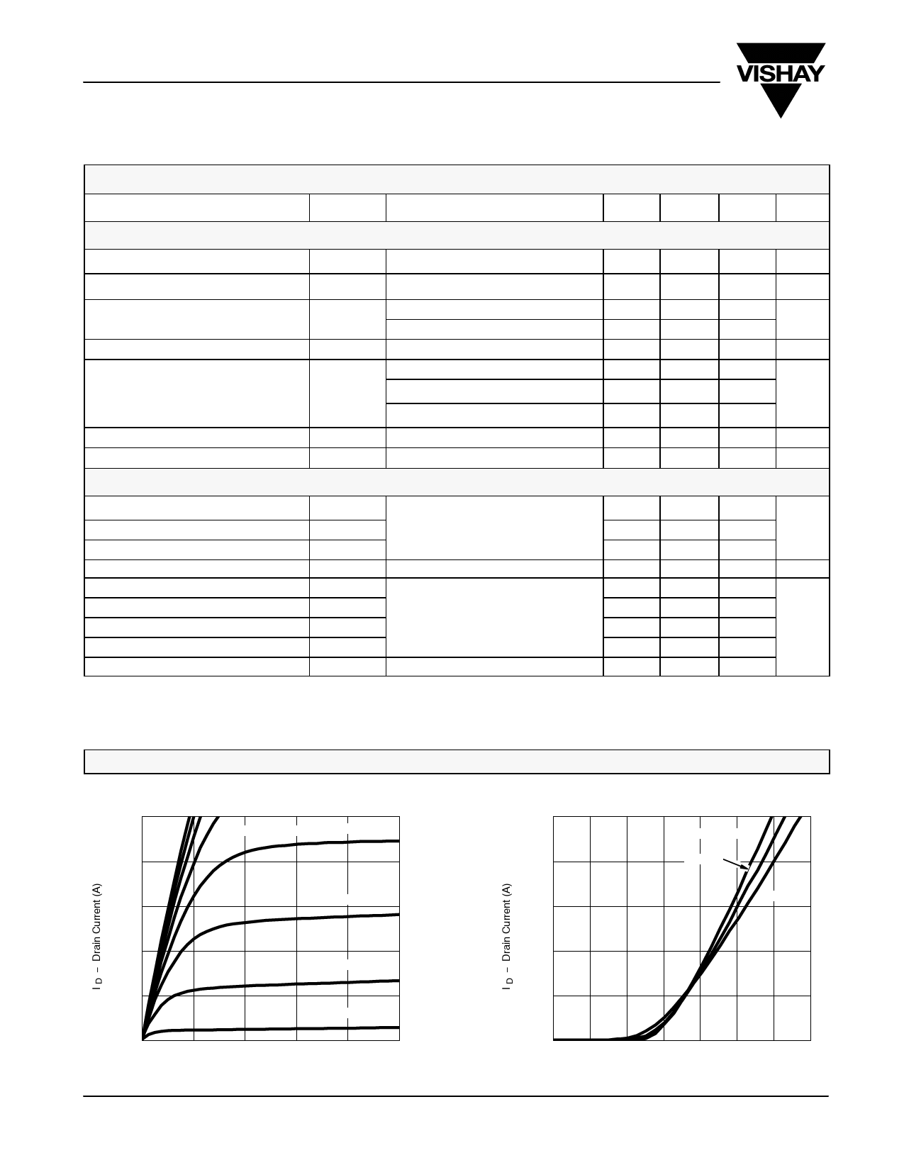
On-State Drain Currenta
Drain-Source On-State Resistancea
Forward Transconductancea
Diode Forward Voltagea
Dynamicb
VGS(th)
IGSS
IDSS
ID(on)
rDS(on)
gfs
VSD
VDS = VGS, ID = –250 mA
VDS = 0 V, VGS = "12 V
VDS = –20 V, VGS = 0 V
VDS = –20 V, VGS = 0 V, TJ = 70_C
VDS = –5 V, VGS = –4.5 V
VGS = –4.5 V, ID = –4.4 A
VGS = –2.7 V, ID = –3.7 A
VGS = –2.5 V, ID = –3.5 A
VDS = –10 V, ID = –4.4 A
IS = –1.7 A, VGS = 0 V
Total Gate Charge
Gate-Source Charge
Gate-Drain Charge
Turn-On Delay Time
Rise Time
Turn-Off Delay Time
Fall Time
Source-Drain Reverse Recovery Time
Qg
Qgs
Qgd
td(on)
tr
td(off)
tf
trr
Notes
a. Pulse test; pulse width v 300 ms, duty cycle v 2%.
b. Guaranteed by design, not subject to production testing.
VDS = –10 V, VGS = –4.5 V, ID = –4.4 A
VDD = –10 V, RL = 10 W
ID ^ –1.0 A, VGEN = –4.5 V, RG = 6 W
IF = –1.7 A, di/dt = 100 A/ms
Min
–0.6
–15
Typ Max Unit
V
"100
nA
–1
mA
–5
A
0.058
0.065
0.080
0.090
W
0.087
0.100
10
S
–1.2
V
8.5
15
2.8
nC
1.7
15
50
32
60
57
100
ns
40
80
40
80
www.vishay.com S FaxBack 408-970-5600
2-2
Document Number: 70713
S-54948—Rev. B, 29-Sep-97
Share Link: 