AD558T Ver la hoja de datos (PDF) - Analog Devices
NГәmero de pieza
componentes DescripciГіn
Fabricante
AD558T Datasheet PDF : 8 Pages
| |||
AD558
OUTPUT
AMP
16
15
VOUT
0.5mA
вҖ“V
VOUT SENSE
14 VOUT SELECT
13
AGND
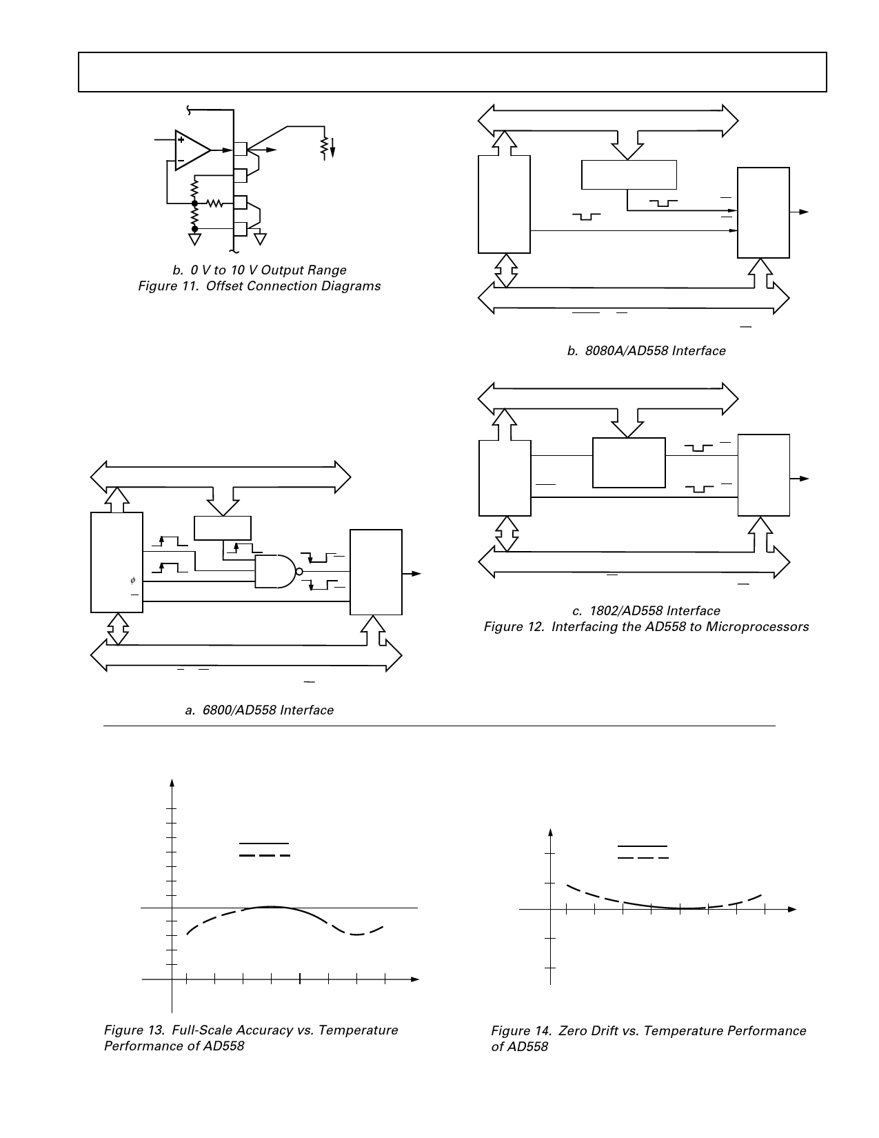
b. 0 V to 10 V Output Range
Figure 11. Offset Connection Diagrams
INTERFACING THE AD558 TO MICROPROCESSOR
DATA BUSES
The AD558 is configured to act like a вҖңwrite onlyвҖқ location in
memory that may be made to coincide with a read only memory
location or with a RAM location. The latter case allows data
previously written into the DAC to be read back later via the
RAM. Address decoding is partially complete for either ROM
or RAM. Figure 12 shows interfaces for three popular micropro-
cessor systems.
16
6800
VMA
ПҶ2
R/W
8
ADDRESS BUS
16
ADDRESS
DECODER
CS
VOUT
AD558
CE
DB0вҖ“DB7
8
DATA BUS
R/W вҶ’ CE
GATED DECODED ADDRESS вҶ’ CS
a. 6800/AD558 Interface
ADDRESS BUS
16
8080A
MEMW
16
ADDRESS SELECT
PULSE LOGIC
CS AD558 VOUT
CE
DB0вҖ“DB7
8
8
DATA BUS
MEMW вҶ’ CE
DECODED ADDRESS SELECT PULSE вҶ’ CS
b. 8080A/AD558 Interface
8
ADDRESS BUS
MA 0 вҖ“ 7
TPA
1802
MWR
8
ADDRESS
LATCH
&
DECODE
CS
AD558 VOUT
CE
DB0вҖ“DB7
8
8
DATA BUS
CDP 1802: MWR вҶ’ CE
DECODED ADDRESS SELECT PULSE вҶ’ CS
c. 1802/AD558 Interface
Figure 12. Interfacing the AD558 to Microprocessors
Performance (typical @ +25ШҮC, VCC ШҺ +5 V to +15 V unless otherwise noted)
LSB
1.75
1.50
1.25
1.00
0.75
0.50
0.25
FULL
SCALE
0
ERROR вҖ“0.25
вҖ“0.50
вҖ“0.75
вҖ“1.00
ALL AD558
AD558S, T
вҖ“55 вҖ“25 0 +25 +50 +75 +100 +125 oC
1LSB = 0.39% OF FULL SCALE
Figure 13. Full-Scale Accuracy vs. Temperature
Performance of AD558
LSB
1/2
ZERO
ERROR
1/4
ALL AD558
AD558S, T
0
вҖ“55 вҖ“25 0 +25 +50 +75 +100 +125 oC
вҖ“1/4
вҖ“1/2
1LSB = 0.39% OF FULL SCALE
Figure 14. Zero Drift vs. Temperature Performance
of AD558
REV. A
вҖ“7вҖ“
Share Link: 