ISL59444 Ver la hoja de datos (PDF) - Renesas Electronics
Número de pieza
componentes Descripción
Fabricante
ISL59444 Datasheet PDF : 13 Pages
| |||
ISL59444
PC Board Layout
The frequency response of this circuit depends greatly on the
care taken in designing the PC board. The following are
recommendations to achieve optimum high frequency
performance from your PC board.
• The use of low inductance components such as chip resistors
and chip capacitors is strongly recommended.
• Minimize signal trace lengths. Trace inductance and
capacitance can easily limit circuit performance. Avoid sharp
corners, use rounded corners when possible. Vias in the signal
lines add inductance at high frequency and should be avoided.
PCB traces greater than 1" begin to exhibit transmission line
characteristics with signal rise/fall times of 1ns or less. High
frequency performance may be degraded for traces greater
than one inch, unless strip lines are used.
• Match channel-channel analog I/O trace lengths and layout
symmetry. This will minimize propagation delay mismatches.
• Maximize use of AC de-coupled PCB layers. All signal I/O lines
should be routed over continuous ground planes (i.e., no split
planes or PCB gaps under these lines). Avoid vias in the signal
I/O lines.
• Use proper value and location of termination resistors.
Termination resistors should be as close to the device as
possible.
• When testing use good quality connectors and cables, matching
cable types and keeping cable lengths to a minimum.
• Minimum of 2 power supply de-coupling capacitors are
recommended (1000pF, 0.01µF) as close to the devices as
possible. Avoid vias between the cap and the device because
vias add unwanted inductance. Larger caps can be farther
away. When vias are required in a layout, they should be routed
as far away from the device as possible.
• The NIC pins are placed on both sides of the input pins. These
pins are not internally connected to the die. It is recommended
these pins be tied to ground to minimize crosstalk.
V+ SUPPLY
LOGIC
POWER
GND
SIGNAL
DE-COUPLING
CAPS
V- SUPPLY
SCHOTTKY
PROTECTION
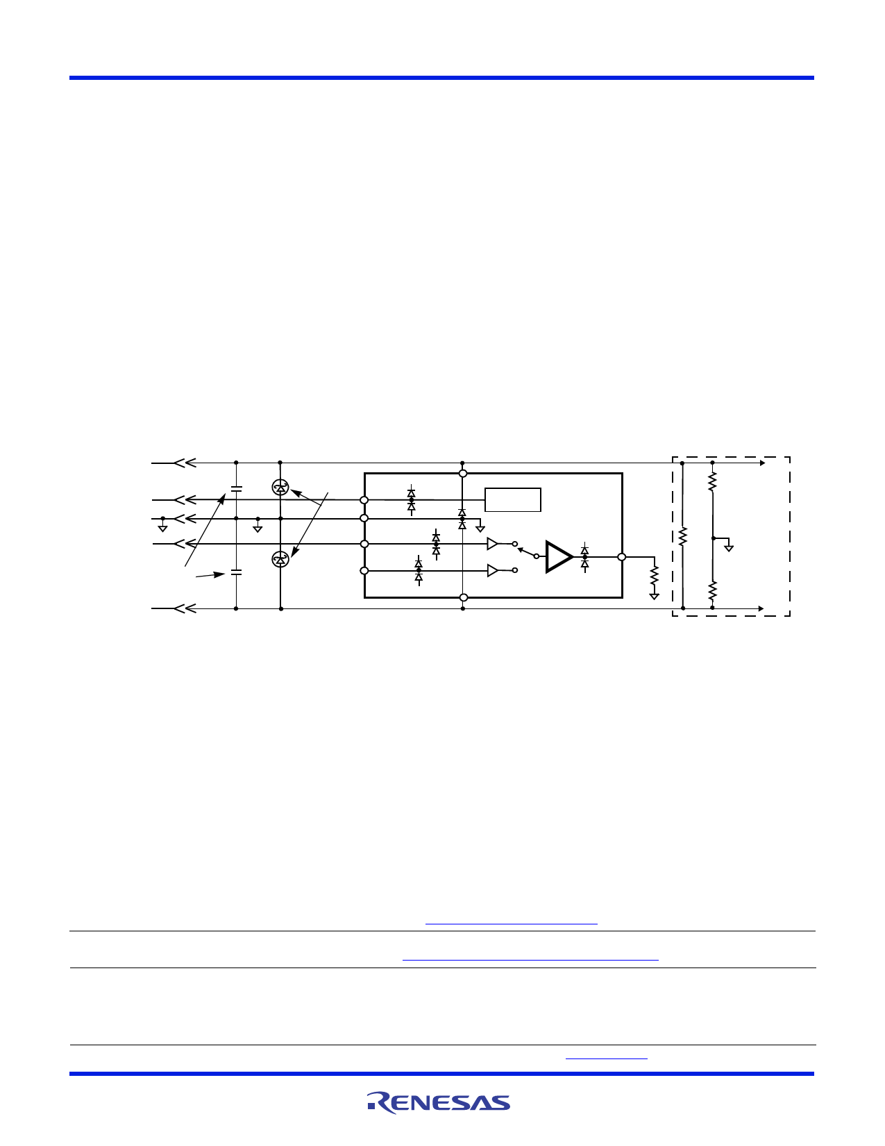
V+
S0
GND V- V+
IN0
V+
V-
IN1
V-
V+
LOGIC
CONTROL
V-
V+
OUT
V-
FIGURE 25. SCHOTTKY PROTECTION CIRCUIT
EXTERNAL
CIRCUITS
© Copyright Intersil Americas LLC 2005-2012. All Rights Reserved.
All trademarks and registered trademarks are the property of their respective owners.
For additional products, see www.intersil.com/en/products.html
Intersil products are manufactured, assembled and tested utilizing ISO9001 quality systems as noted
in the quality certifications found at www.intersil.com/en/support/qualandreliability.html
Intersil products are sold by description only. Intersil may modify the circuit design and/or specifications of products at any time without notice, provided that such
modification does not, in Intersil's sole judgment, affect the form, fit or function of the product. Accordingly, the reader is cautioned to verify that datasheets are
current before placing orders. Information furnished by Intersil is believed to be accurate and reliable. However, no responsibility is assumed by Intersil or its
subsidiaries for its use; nor for any infringements of patents or other rights of third parties which may result from its use. No license is granted by implication or
otherwise under any patent or patent rights of Intersil or its subsidiaries.
For information regarding Intersil Corporation and its products, see www.intersil.com
FN7451 Rev 3.00
August 16, 2012
Page 12 of 13
Share Link: 