ISL59450 Ver la hoja de datos (PDF) - Renesas Electronics
Número de pieza
componentes Descripción
Fabricante
ISL59450 Datasheet PDF : 37 Pages
| |||
ISL59450
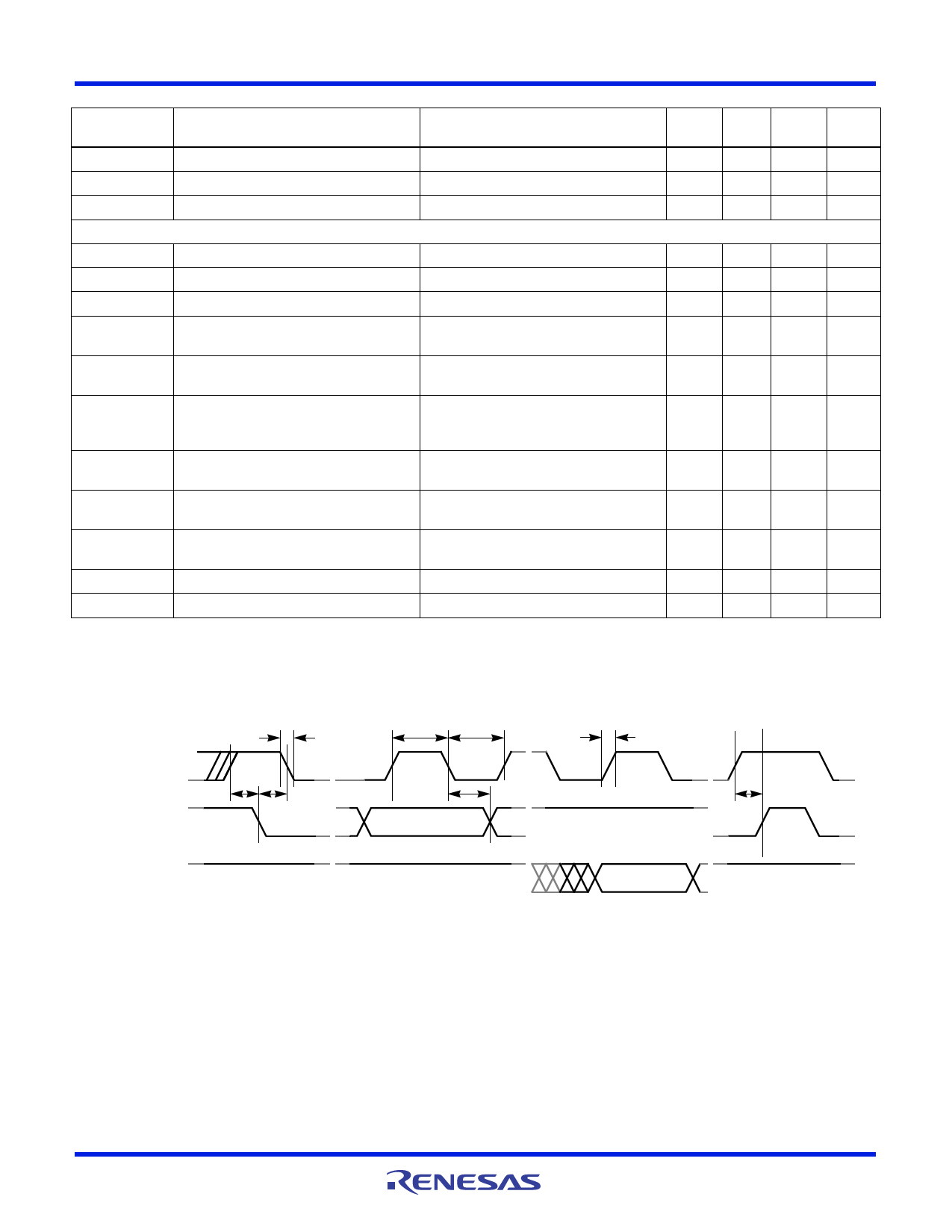
Serial Interface (I2C) Specifications
SYMBOL
PARAMETER
CONDITIONS
MIN
(Note 1) TYP
VOL
SDA Output Buffer LOW Voltage
ILI
Input Leakage Current on SCL
ILO
I/O Leakage Current on SDA
TIMING CHARACTERISTICS
IOL = 4mA
VIN = 5.5V
VIN = 5.5V
0
0.1
0.1
fSCL
tLOW
tHIGH
tSU:STA
tHD:STA
tHD:DAT
SCL Frequency
Clock LOW Time
Clock HIGH Time
START Condition Set-up Time
START Condition Hold Time
Input Data Hold Time
Measured at the 30% of VD crossing.
1.3
Measured at the 70% of VD crossing.
0
SCL rising edge to SDA falling edge. Both 0.6
crossing 70% of VD.
From SDA falling edge crossing 30% of VD 0.6
to SCL falling edge crossing 70% of VD.
From SCL falling edge crossing 70% of VD
0
to SDA entering the 30% to 70% of VD
window.
tSU:STO
tR
STOP Condition Set-up Time
SDA and SCL Rise Time
From SCL rising edge crossing 70% of VD,
to SDA rising edge crossing 30% of VD
From 30% to 70% of VD
0.6
20 +
0.1 x Cb
tF
SDA and SCL Fall Time
From 70% to 30% of VD
20 +
0.1 x Cb
Cb
Capacitive Loading of SDA or SCL
Total on-chip and off-chip
Cpin
SDA and SCL Pin Capacitance
NOTE:
1. Parts are 100% tested at +25°C. Temperature limits established by characterization and are not production tested.
MAX
(Note 1)
0.4
1
1
400
0.9
0.9
400
10
UNIT
V
µA
µA
kHz
µs
µs
µs
µs
µs
µs
ns
ns
pF
pF
I2C Timing Diagram
tF
tHIGH
tLOW
tR
SCL
tSU:STA
SDA
(INPUT TIMING)
tHD:STA
tHD:DAT
tSU:STO
SDA
(OUTPUT TIMING)
FN7510 Rev 0.00
Feb 14, 2008
Page 5 of 37
Share Link: 