OPAMPSOT23EVAL Ver la hoja de datos (PDF) - Renesas Electronics
Número de pieza
componentes Descripción
Fabricante
OPAMPSOT23EVAL
Renesas Electronics
OPAMPSOT23EVAL Datasheet PDF : 11 Pages
| |||
HFA1150
50
AV = +2
40
30
20
SOIC
10
SOT-23
0
0 50 100 150 200 250 300 350 400
LOAD CAPACITANCE (pF)
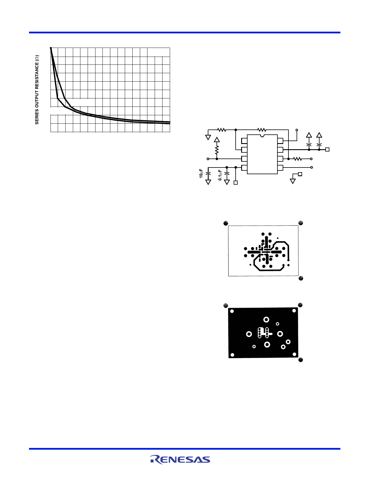
FIGURE 1. RECOMMENDED SERIES OUTPUT RESISTOR vs
LOAD CAPACITANCE
PC Board Layout
The frequency response of this amplifier depends greatly on
the amount of care taken in designing the PC board. The use
of low inductance components such as chip resistors and
chip capacitors is strongly recommended, while a solid
ground plane is a must!
Attention should be given to decoupling the power supplies. A
large value (10F) tantalum in parallel with a small value chip
(0.1F) capacitor works well in most cases.
Terminated microstrip signal lines are recommended at the
input and output of the device. Output capacitance, such as
that resulting from an improperly terminated transmission line,
will degrade the frequency response of the amplifier and may
cause oscillations. In most cases, the oscillation can be
avoided by placing a resistor in series with the output.
Care must also be taken to minimize the capacitance to ground
seen by the amplifier’s inverting input. The larger this capacitance,
the worse the gain peaking, resulting in pulse overshoot and
eventual instability. To reduce this capacitance, remove the
ground plane under traces connected to -IN and keep these
traces as short as possible.
Examples of good high frequency layouts are the evaluation
boards shown below.
Evaluation Boards
The performance of the HFA1150IB (SOIC) may be evaluated
using the HFA11XX Evaluation Board and a SOIC to DIP
adaptor like the Aries Electronics Part Number
08-350000-10. The SOT-23 version can be evaluated using
the OPAMPSOT23EVAL board.
To order evaluation boards (part number HFA11XXEVAL or
OPAMPSOT23EVAL), please contact your local sales office.
The schematic and layout of the HFA11XXEVAL and
OPAMPSOT23EVAL boards are shown below.
511
511
NC
1
50
2
IN
3
4
-5V
8
7
6
5
GND
0.1F
10F
50
+5V
OUT
NC
GND
FIGURE 2. HFA11XXEVAL SCHEMATIC
HFA11XXEVAL TOP LAYOUT
VH
1
+IN
VL V-
V+
GND
HFA11XXEVAL BOTTOM LAYOUT
FN4836 Rev 1.00
June 2004
Page 5 of 11
Share Link: 