MJ11021G(2008) データシートの表示(PDF) - ON Semiconductor
部品番号
コンポーネント説明
メーカー
MJ11021G Datasheet PDF : 5 Pages
| |||
MJ11021(PNP) MJ11022 (NPN)
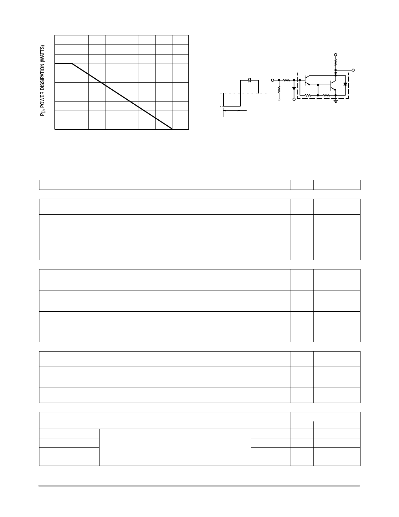
RB and RC VARIED TO OBTAIN DESIRED CURRENT LEVELS
200
D1 MUST BE FAST RECOVERY TYPE, e.g.:
VCC
1N5825 USED ABOVE IB ≈ 100 mA
100 V
MSD6100 USED BELOW IB ≈ 100 mA
RC SCOPE
TUT
150
V2
RB
APPROX
100
+12 V
0
51
D1
≈ 10 K ≈ 8.0
V1
APPROX
+ 4.0 V
50
- 8.0 V
25 ms
for td and tr, D1 is disconnected
and V2 = 0
0
0 25 50 75 100 125 150 175 200
TC, CASE TEMPERATURE (°C)
tr, tf ≤ 10 ns
DUTY CYCLE = 1.0%
For NPN test circuit reverse diode and voltage polarities.
Figure 1. Power Derating
Figure 2. Switching Times Test Circuit
ELECTRICAL CHARACTERISTICS (TC = 25_C unless otherwise noted)
Characteristic
OFF CHARACTERISTICS
Collector−Emitter Sustaining Voltage (Note 1)
(IC = 0.1 Adc, IB = 0)
Collector Cutoff Current
(VCE = 125, IB = 0)
Collector Cutoff Current
(VCE = Rated VCB, VBE(off) = 1.5 Vdc)
(VCE = Rated VCB, VBE(off) = 1.5 Vdc, TJ = 150_C)
Emitter Cutoff Current (VBE = 5.0 Vdc, IC = 0)
ON CHARACTERISTICS (Note 1)
MJ11021, MJ11022
MJ11021, MJ11022
DC Current Gain
(IC = 10 Adc, VCE = 5.0 Vdc)
(IC = 15 Adc, VCE = 5.0 Vdc)
Collector−Emitter Saturation Voltage
(IC = 10 Adc, IB = 100 mA)
(IC = 15 Adc, IB = 150 mA)
Base−Emitter On Voltage
IC = 10 A, VCE = 5.0 Vdc)
Base−Emitter Saturation Voltage
(IC = 15 Adc, IB = 150 mA)
DYNAMIC CHARACTERISTICS
Current−Gain Bandwidth Product
(IC = 10 Adc, VCE = 3.0 Vdc, f = 1.0 MHz)
Output Capacitance (VCB = 10 Vdc, IE = 0, f = 0.1 MHz)
MJ11022
MJ11021
Small−Signal Current Gain
(IC = 10 Adc, VCE = 3.0 Vdc, f = 1.0 kHz)
SWITCHING CHARACTERISTICS
Symbol
VCEO(sus)
ICEO
ICEV
IEBO
hFE
VCE(sat)
VBE(on)
VBE(sat)
[hfe]
Cob
hfe
Characteristic
Delay Time
Rise Time
Storage Time
(VCC = 100 V, IC = 10 A, IB = 100 mA
VBE(off) = 50 V) (See Figure 2)
Fall Time
1. Pulsed Test: Pulse Width = 300 ms, Duty Cycle v 2%.
Symbol
td
tr
ts
tf
Min
Max
Unit
Vdc
250
−
mAdc
−
1.0
mAdc
−
0.5
−
5.0
−
2.0 mAdc
−
400 15,000
100
−
Vdc
−
2.0
−
3.4
−
2.8
Vdc
−
3.8
Vdc
3.0
−
Mhz
pF
−
400
−
600
75
−
−
Typical
NPN PNP Unit
150
75
ns
1.2
0.5
ms
4.4
2.7
ms
10.0
2.5
ms
http://onsemi.com
2
Share Link: 