UPD78P368AKL-S データシートの表示(PDF) - NEC => Renesas Technology
部品番号
コンポーネント説明
メーカー
UPD78P368AKL-S Datasheet PDF : 52 Pages
| |||
mPD78P368A
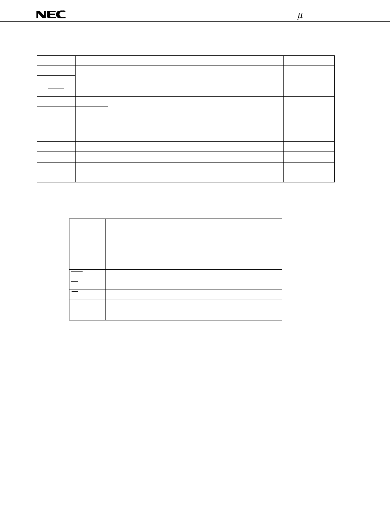
(2) Non-port pins (2/2)
Pin name
MODE0
MODE1
RESET
X1
X2
AVREF
AVDD
AVSS
VDD
VSS
IC
I/O
Function
Dual-function pin
I
Input for the control signal which sets the operation mode. Normally, both
–
MODE0 and MODE1 are directly connected to the VSS pin.
I
System reset input
–
I
Crystal input pin for the system clock. A clock signal provided externally is
–
–
input to the X1 pin. The reversed signal of the clock signal is input to the
X2 pin.
I
A/D converter reference voltage input
–
–
Analog power supply for the A/D converter
–
–
Ground for the A/D converter
–
–
Positive power supply
–
–
Ground
–
–
Internally connected. Directly connect the IC pin to VSS.
–
1.2 PROM PROGRAMMING MODE (MODE0/VPP = H, MODE1 = L)
Pin name
MODE0/VPP
MODE1
A0-A16
D0-D7
PGM
CE
OE
VDD
VSS
I/O
Function
I PROM programming mode set/programming supply voltage
I PROM programming mode set
I Address bus
I/O Data bus
I Program input
I Enable PROM
I Read strobe to PROM
Positive power supply
GND
10
Share Link: 