SPT5216 データシートの表示(PDF) - Signal Processing Technologies
部品番号
コンポーネント説明
メーカー
SPT5216 Datasheet PDF : 10 Pages
| |||
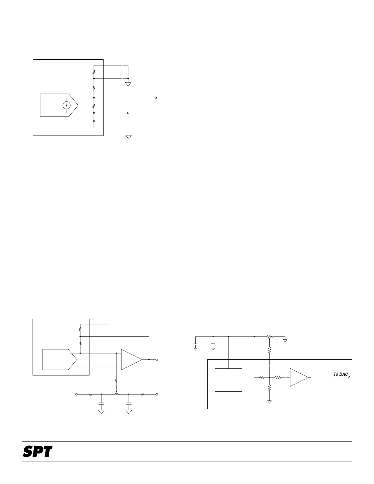
Figure 3 - Connection of Internal Load Resistors for Passive
Unipolar/Bipolar Current-to-Voltage Conversion
For Bipolar Mode Only
BPO
DAC
0-5 mA
1 kΩ
1 kΩ
1 kΩ
Leave Open For
Bipolar Mode
10 V FSR
5 V FSR
DAC Out
DAC RTN
Sense
DAC RTN 1
DAC RTN 2
VOUT
(To High Impedance Load)
AGND
OUTPUT OFFSET COMPENSATION
Although the zero offset error of the SPT5216 is within ±0.1%
of the full scale range, some applications require better
accuracy. The offset trim network of figure 4 shown con-
nected to DAC OUT allows offset adjustment in excess of
±0.2%. This trim network can be used for the active I-to-V
conversion network of figure 2 or the passive circuit of
figure 3. When using an external op amp as in figure 2,
optimum offset stability may be achieved by using the nulling
network recommended by the op amp's manufacturer.
Although accuracy of the offset network components is not
important, temperature tracking of the resistor and potenti-
ometer values will affect offset trim stability. The resistors and
potentiometer should have a low temperature coefficient and
the potentiometer should be a high quality, multi-turn compo-
nent to ensure minute adjustability and stability over time and
temperature. The 0.1 µF capacitors shown (typically ce-
ramic) are used to decouple power supply noise from the
DAC output circuit.
LOGIC INTERFACE
Because of the low logic input current specification, most
high-speed CMOS logic families will adequately drive the
SPT5216. Nonadherence to the VIH specification will result in
a less than specified DAC accuracy. High-speed CMOS logic
(HC), high-speed CMOS logic with TTL-compatible outputs
(HCT) or TTL logic with open-collector outputs are directly
compatible with the SPT5216 logic inputs.
GAIN ADJUSTMENT
With the gain error of the SPT5216 pre-trimmed to within
±0.15% of full scale accuracy, many applications require
external gain adjustments. Configuration of the external gain
adjustment network is shown is figure 5. The adjustment
potentiometer is connected between two low noise voltage
sources, REF OUT and AGND, as shown. The two bypass
capacitors shown further help to eliminate noise. Because of
the voltage source asymmetry in relationship to the potenti-
ometer wiper, the adjustment range is an asymmetric -0.6%
to +1%. This adjustment range does sufficiently compensate
for the error of the device, and the network will work for any
type of output configuration. The adjustment range can be
made larger and symmetrical by using a circuit similar to the
offset compensation network as shown in figure 4, but with
the consequence of introducing power supply noise (and
power supply variations) into the vital voltage reference
circuit.
The selection criteria for the gain adjustment network compo-
nents is similar to those described for the offset compensa-
tion network. Accuracy is not as important as temperature
stability.
Figure 4 - Offset Compensation
10 V FSR
5 V FSR
DAC
DAC Out
DAC RTN
Sense
-
OP AMP
+
470 kΩ
+15 V
10 kΩ
0.1 µF
10 kΩ
10 kΩ
0.1 µF
VOUT
-15 V
Figure 5 - Gain Trim Network Suitable for All Output
Configurations
+
15 µF
0.01 µF
Ref Out
Ref In
10 kΩ
AGND
330 kΩ
Gain Adj
5 Volt
Bandgap
Voltage
Reference
Gain
Adj
Circuit
gm
AMP
Switch
Bias
To DAC
Network
AGND
AGND
SPT
6
SPT5216
3/4/97
Share Link: 