DMC16249HB データシートの表示(PDF) - Optrex Corporation
部品番号
コンポーネント説明
メーカー
DMC16249HB Datasheet PDF : 15 Pages
| |||
4.I/O Terminal
4.1.Pin Assignment
No.
Symbol
1
VSS
2
VCC
3
VEE
4
RS
5
R/W
6
E
7
DB0
8
DB1
9
DB2
10
DB3
11
DB4
12
DB5
13
DB6
14
DB7
Level
-
-
-
H/L
H/L
H/L
H/L
H/L
H/L
H/L
H/L
H/L
H/L
H/L
Function
Power Supply (0V, GND)
Power Supply for Logic
Power Supply for LCD Drive
Register Select Signal
Read/Write Select Signal H : Read L : Write
Enable Signal (No pull-up Resister)
Data Bus Line / Non-connection at 4-bit operation
Data Bus Line / Non-connection at 4-bit operation
Data Bus Line / Non-connection at 4-bit operation
Data Bus Line / Non-connection at 4-bit operation
Data Bus Line
Data Bus Line
Data Bus Line
Data Bus Line
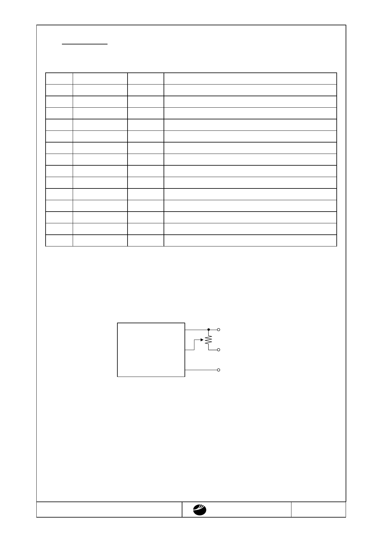
4.2.Example of Power Supply
It is recommended to apply a potentiometer for the contrast adjust due to the tolerance
of the driving voltage and its temperature dependence.
VCC
VR
MODULE VEE
VSS
VR=10~20KΩ
VCC (+Voltage)
VEE (-Voltage)
VSS (0V)
DMC16249HB* (BE) No.99-0325
OPTREX CORPORATION
OPTREX
Page 7/15
Share Link: 