74AHC595 データシートの表示(PDF) - Philips Electronics
部品番号
コンポーネント説明
メーカー
74AHC595
Philips Electronics
74AHC595 Datasheet PDF : 20 Pages
| |||
Philips Semiconductors
8-bit serial-in/serial or parallel-out shift
register with output latches; 3-state
Product specification
74AHC595; 74AHCT595
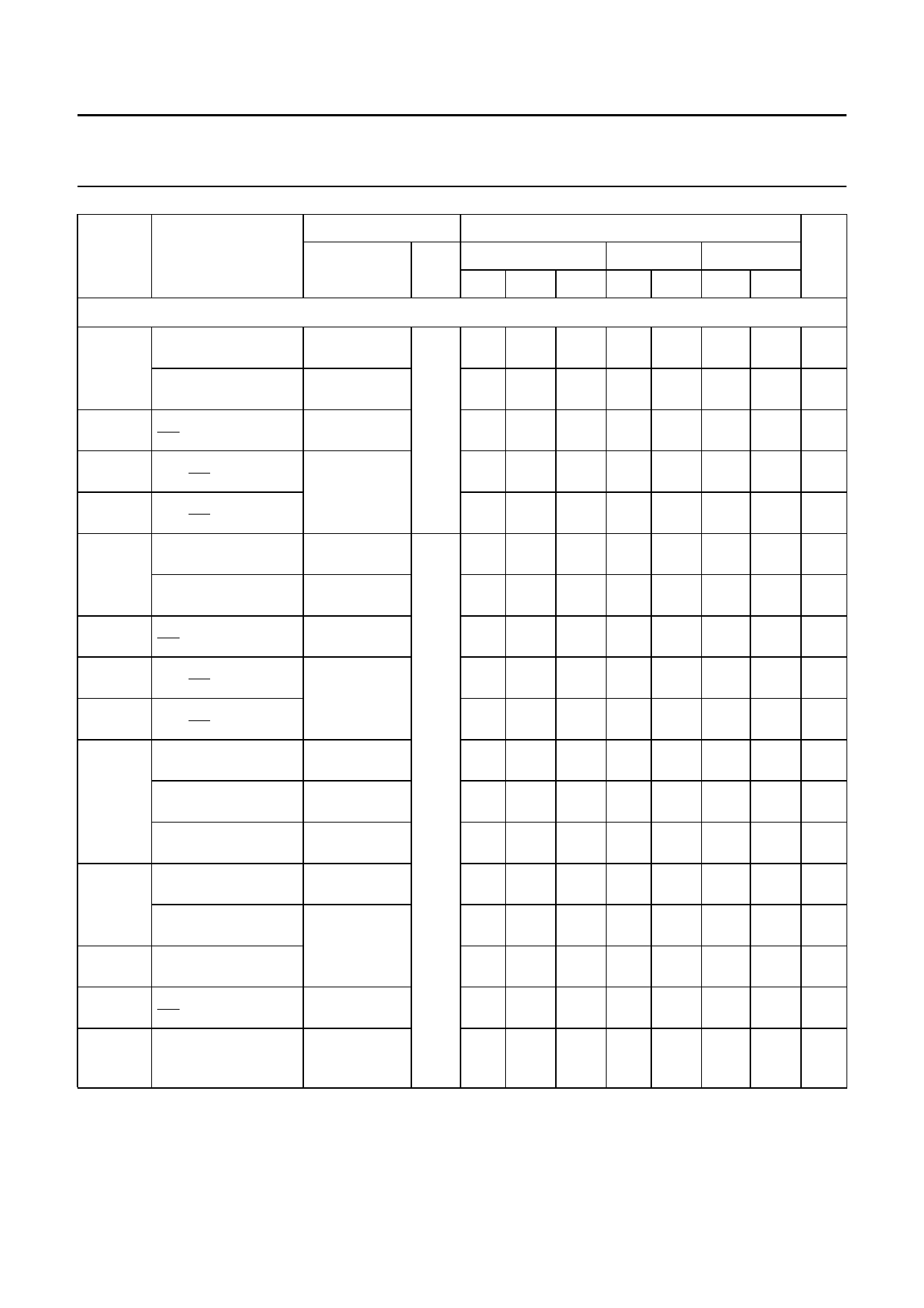
SYMBOL
PARAMETER
TEST CONDITIONS
WAVEFORMS CL
MIN.
25
TYP.
Tamb (°C)
−40 to +85
−40 to +125 UNIT
MAX. MIN. MAX. MIN. MAX.
VCC = 4.5 to 5.5 V; note 2
tPHL/tPLH
tPHL
tPZH/tPZL
tPHZ/tPLZ
tPHL/tPLH
tPHL
tPZH/tPZL
tPHZ/tPLZ
tW
propagation delay
SHCP to Q7’
propagation delay
STCP to Qn
propagation delay
MR to Q7’
3-state output enable
time OE to Qn
3-state output disable
time OE to Qn
propagation delay
SHCP to Q7’
propagation delay
STCP to Qn
propagation delay
MR to Q7’
3-state output enable
time OE to Qn
3-state output disable
time OE to Qn
shift clock pulse width
HIGH or LOW
see Figs 7
and 12
see Figs 8
and 12
see Figs 10
and 12
see Figs 11
and 12
see Figs 7
and 12
see Figs 8
and 12
see Figs 10
and 12
see Figs 11
and 12
see Figs 7
and 12
storage clock pulse see Figs 8
width HIGH or LOW and 12
master reset pulse
width LOW
see Figs 10
and 12
tsu
set-up time
DS to SHCP
see Figs 8
and 12
set-up time
see Figs 9
SHCP to STCP
and 12
th
hold time
DS to SHCP
trem
removal time
MR to SHCP
see Figs 10
and 12
fmax
maximum clock pulse see Figs 7, 8
frequency
and 12
SHCP or STCP
Notes
1. Typical values at VCC = 3.3 V.
2. Typical values at VCC = 5.0 V.
15 pF −
4.0
−
4.2
−
4.4
−
4.0
−
3.8
50 pF −
5.4
−
5.5
−
5.6
−
5.3
−
5.8
5.0 −
5.0 −
5.0 −
3.0 −
5.0 −
2.0 −
2.5 −
130 170
8.2
7.4
8.0
8.6
8.0
10.0
9.0
10.0
10.6
10.3
−
−
−
−
−
−
−
−
1.0 9.4 1.0
1.0 8.5 1.0
1.0 9.1 1.0
1.0 10.0 1.0
1.0 9.5 1.0
1.0 11.4 1.0
1.0 10.5 1.0
1.0 11.1 1.0
1.0 12.0 1.0
1.0 11.0 1.0
5.0 −
5.0
5.0 −
5.0
5.0 −
5.0
3.0 −
3.0
5.0 −
5.0
2.0 −
2.0
2.5 −
2.5
110 −
90
10.5 ns
9.5 ns
10.0 ns
11.0 ns
10.5 ns
12.5 ns
11.5 ns
12.0 ns
13.0 ns
12.0 ns
−
ns
−
ns
−
ns
−
ns
−
ns
−
ns
−
ns
−
MHz
2000 Mar 15
11
Share Link: 