OP27G データシートの表示(PDF) - Analog Devices
部品番号
コンポーネント説明
メーカー
OP27G Datasheet PDF : 22 Pages
| |||
OP27
For reference, typical source resistances of some signal sources
are listed in Table 7.
Table 7.
Device
Strain Gauge
Magnetic
Tape Head
Magnetic
Phonograph
Cartridges
Linear
Variable
Differential
Transformer
Source
Impedance
<500 Ω
<1500 Ω
<1500 Ω
<1500 Ω
Comments
Typically used in low frequency
applications.
Low is very important to reduce
self-magnetization problems
when direct coupling is used.
OP27 IB can be neglected.
Similar need for low IB in direct
coupled applications. OP27 does
not introduce any self-
magnetization problems.
Used in rugged servo-feedback
applications. Bandwidth of
interest is 400 Hz to 5 kHz.
Table 8. Open-Loop Gain
Frequency
OP07
At 3 Hz
100 dB
At 10 Hz
100 dB
At 30 Hz
90 dB
OP27
124 dB
120 dB
110 dB
OP37
125 dB
125 dB
124 dB
AUDIO APPLICATIONS
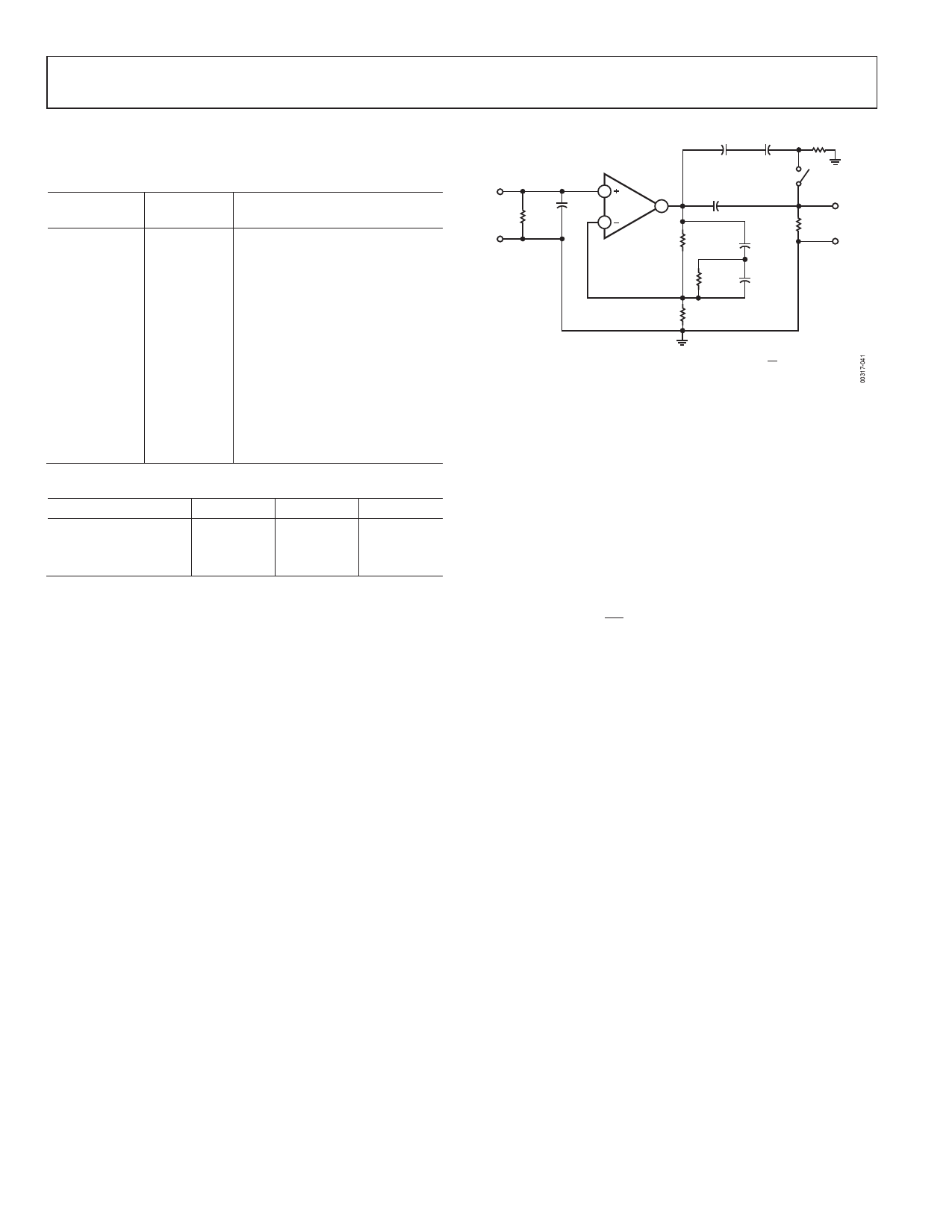
Figure 41 is an example of a phono pre-amplifier circuit using the
OP27 for A1; R1-R2-C1-C2 form a very accurate RIAA network
with standard component values. The popular method to
accomplish RIAA phono equalization is to employ frequency
dependent feedback around a high quality gain block. Properly
chosen, an RC network can provide the three necessary time
constants of 3180 µs, 318 µs, and 75 µs.
For initial equalization accuracy and stability, precision metal
film resistors and film capacitors of polystyrene or polypro-
pylene are recommended because they have low voltage
coefficients, dissipation factors, and dielectric absorption.
(High-k ceramic capacitors should be avoided here, though
low-k ceramics, such as NPO types that have excellent
dissipation factors and somewhat lower dielectric absorption,
can be considered for small values.)
Data Sheet
C4 (2)
+220µF +
R5
N
MOVING MAGNET
CARTRIDGE INPUT
3
RA
CA
150pF
A1
OP27
6
N
2
LF ROLLOFF
C3
OUT IN
0.47µF
R1
N
R4
N
C1
0.03µF
OUTPUT
R2
N
C2
0.01µF
R3
G = 1kHz GAIN
= 0.101 ( 1 + R1 )
R3
= 98.677 (39.9dB) AS SHOWN
Figure 41. Phono Preamplifier Circuit
The OP27 brings a 3.2 nV/√Hz voltage noise and 0.45 pA/√Hz
current noise to this circuit. To minimize noise from other
sources, R3 is set to a value of 100 Ω, generating a voltage noise
of 1.3 nV/√Hz. The noise increases the 3.2 nV/√Hz of the
amplifier by only 0.7 dB. With a 1 kΩ source, the circuit noise
measures 63 dB below a 1 mV reference level, unweighted, in a
20 kHz noise bandwidth.
Gain (G) of the circuit at 1 kHz can be calculated by the
expression:
G
0.101 ¨©§1
R1
R3
¸¹·
For the values shown, the gain is just under 100 (or 40 dB).
Lower gains can be accommodated by increasing R3, but gains
higher than 40 dB show more equalization errors because of the
8 MHz gain bandwidth of the OP27.
This circuit is capable of very low distortion over its entire
range, generally below 0.01% at levels up to 7 V rms. At 3 V
output levels, it produces less than 0.03% total harmonic
distortion at frequencies up to 20 kHz.
Capacitor C3 and Resistor R4 form a simple −6 dB per octave
rumble filter, with a corner at 22 Hz. As an option, the switch
selected Shunt Capacitor C4, a nonpolarized electrolytic,
bypasses the low frequency roll-off. Placing the rumble filter’s
high-pass action after the preamplifier has the desirable result
of discriminating against the RIAA-amplified low frequency
noise components and pickup produced low frequency
disturbances.
A preamplifier for NAB tape playback is similar to an RIAA
phono preamplifier, though more gain is typically demanded,
along with equalization requiring a heavy low frequency boost.
The circuit in Figure 41 can be readily modified for tape use, as
shown by Figure 42.
Rev. H | Page 16 of 21
Share Link: 