AD542 データシートの表示(PDF) - Analog Devices
部品番号
コンポーネント説明
メーカー
AD542 Datasheet PDF : 12 Pages
| |||
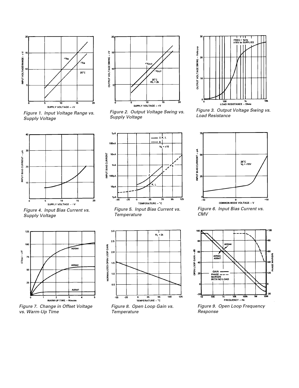
AD542/AD544/AD547–Typical Characteristics
Figure 1. Input Voltage Range vs.
Supply Voltage
Figure 2. Output Voltage Swing vs.
Supply Voltage
Figure 3. Output Voltage Swing vs.
Load Resistance
Figure 4. Input Bias Current vs.
Supply Voltage
Figure 5. Input Bias Current vs.
Temperature
Figure 6. Input Bias Current vs.
CMV
Figure 7. Change in Offset Voltage
vs. Warm-Up Time
Figure 8. Open Loop Gain vs.
Temperature
Figure 9. Open Loop Frequency
Response
–4–
REV. B
Share Link: 