APL1117A データシートの表示(PDF) - Anpec Electronics
部品番号
コンポーネント説明
メーカー
APL1117A Datasheet PDF : 13 Pages
| |||
APL1117A
Pin Description
PIN
NO.
NAME
FUNCTION
1
ADJ (GND)
A resistor divider from this pin to the VOUT pin and ground sets the output voltage. (GND only for
Fixed-Mode)
2
VOUT
The output of the regulator. A minimum of 10µF capacitor (0.15Ω≤ ESR ≤20Ω) must be connected from
this pin to the ground to insure stability
The input pin of regulator. Typically a large storage capacitor (0.15Ω≤ ESR ≤20Ω) is connected from this
3
VIN
pin to the ground to insure that the input voltage does not sag below the minimum dropout voltage during
the load transient response. This pin must always be 1.4V higher than VOUT in order for the device to
regulator properly.
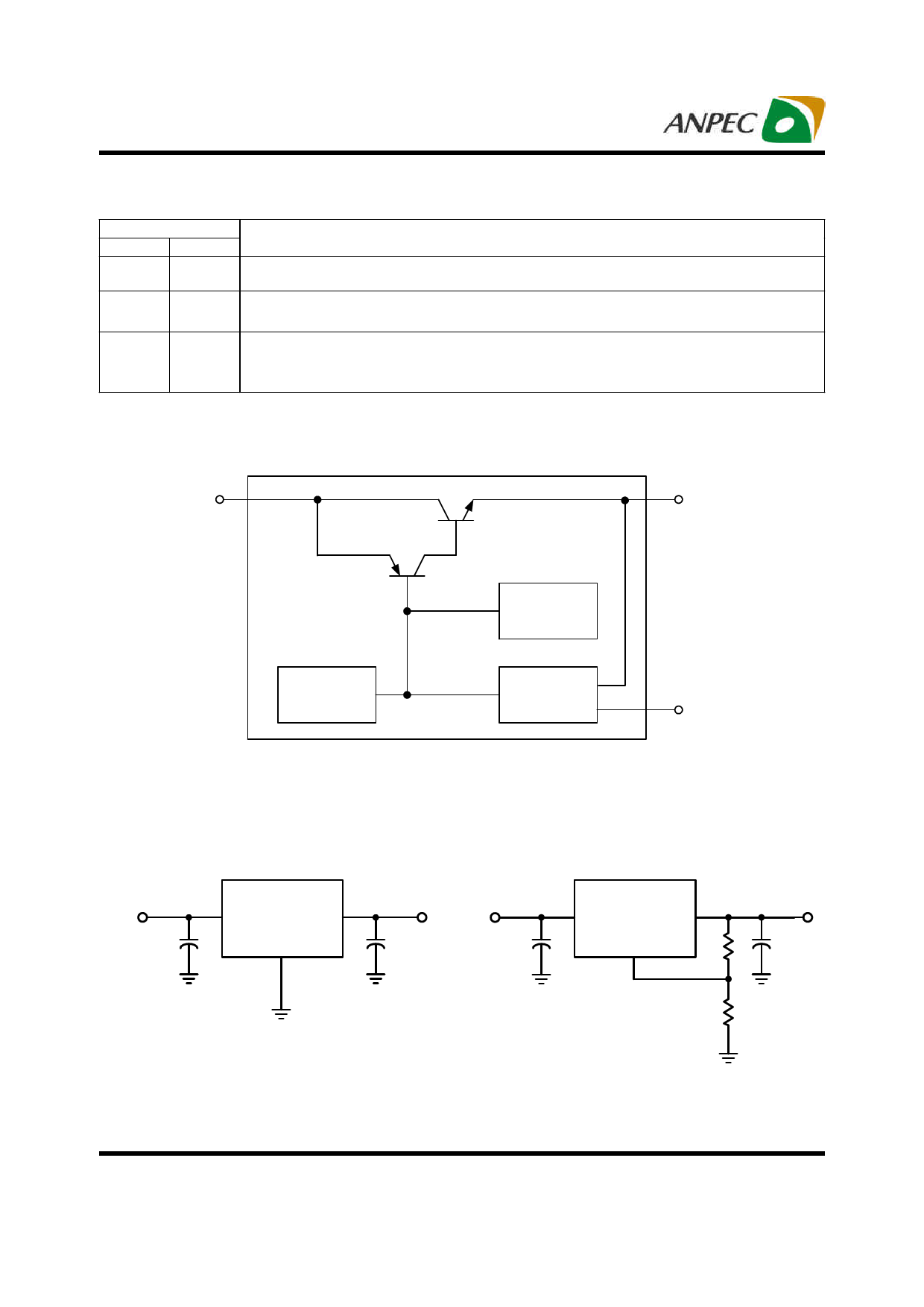
Block Diagram
VIN
VOUT
Thermal
Shutdown
Current Limit
Voltage
Regulation
ADJ/GND
Typical Application Circuits
APL1117A-Fixed
VIN
3 VIN
C1
10~100µF
VOUT
GND
1
VOUT
2
C2
10~100µF
APL1117A-Adj
VIN
3 VIN
C1
10~100µF
VOUT 2
ADJ
R1
1
R2
VOUT
C2
10~100µF
Copyright © ANPEC Electronics Corp.
Rev. A.4 - May., 2010
VOUT = 1.250V X (1 + R2/R1)
VREF / R2 must be greater than 10mA
5
www.anpec.com.tw
Share Link: 