AT45DB021A „Éá„Éľ„āŅ„ā∑„Éľ„Éą„ĀģŤ°®Á§ļÔľąPDFÔľČ - Atmel Corporation
ťÉ®ŚďĀÁē™ŚŹ∑
„ā≥„É≥„ÉĚ„Éľ„Éć„É≥„ÉąŤ™¨śėé
„É°„Éľ„āę„Éľ
AT45DB021A Datasheet PDF : 28 Pages
| |||
memories that are accessed randomly with multiple
address lines and a parallel interface, the DataFlash uses a
serial interface to sequentially access its data. The simple
serial interface facilitates hardware layout, increases sys-
tem reliability, minimizes switching noise, and reduces
package size and active pin count. The device is optimized
for use in many commercial and industrial applications
where high density, low pin count, low voltage, and low
power are essential. Typical applications for the DataFlash
are digital voice storage, image storage, and data storage.
The device operates at clock frequencies up to 13 MHz
with a typical active read current consumption of 4 mA.
To allow for simple in-system reprogrammability, the
AT45DB021A does not require high input voltages for pro-
gramming. The device operates from a single power
supply, 2.7V to 3.6V, for both the program and read opera-
tions. The AT45DB021A is enabled through the chip select
pin (CS) and accessed via a three-wire interface consisting
of the Serial Input (SI), Serial Output (SO), and the Serial
Clock (SCK).
All programming cycles are self-timed, and no separate
erase cycle is required before programming.
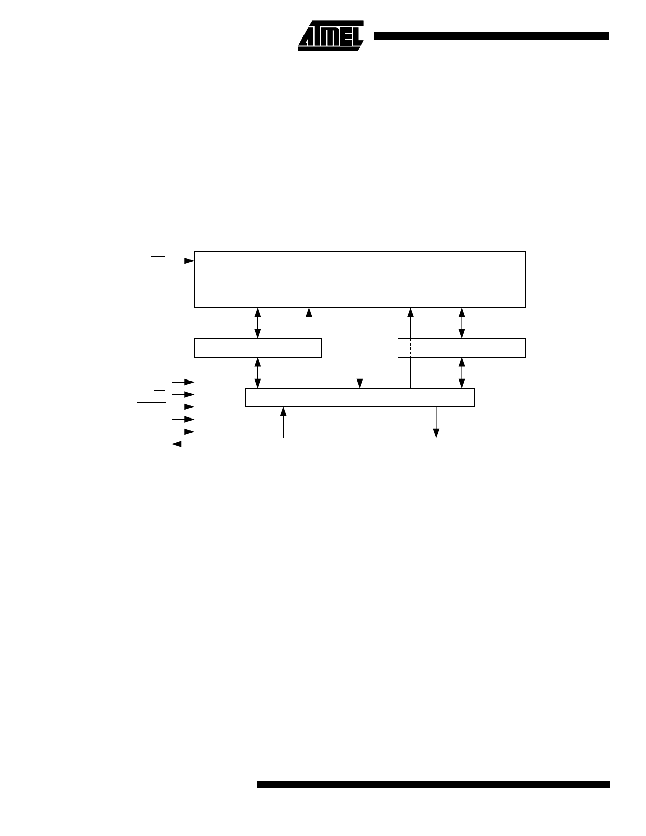
Block Diagram
WP
FLASH MEMORY ARRAY
PAGE (264 BYTES)
BUFFER 1 (264 BYTES)
BUFFER 2 (264 BYTES)
SCK
CS
RESET
VCC
GND
RDY/BUSY
I/O INTERFACE
SI
SO
Memory Array
To provide optimal flexibility, the memory array of the
AT45DB021A is divided into three levels of granularity
comprised of sectors, blocks and pages. The Memory
Architecture Diagram illustrates the breakdown of each
level and details the number of pages per sector and block.
All program operations to the DataFlash occur on a page-
by-page basis; however, the optional erase operations can
be performed at the block or page level.
2
AT45DB021A
Share Link: 