BYS10-35-E3(2008) データシートの表示(PDF) - Vishay Semiconductors
部品番号
コンポーネント説明
メーカー
BYS10-35-E3 Datasheet PDF : 4 Pages
| |||
BYS10-25 thru BYS10-45
Vishay General Semiconductor
2.0
VR = VRRM, Half Sine-Wave, RthJA = 25 K/W
1.6
1.2
BYS10-25
0.8
BYS10-35
0.4
0
0
BYS10-45
40
80
120
160
200
Ambient Temperature (°C)
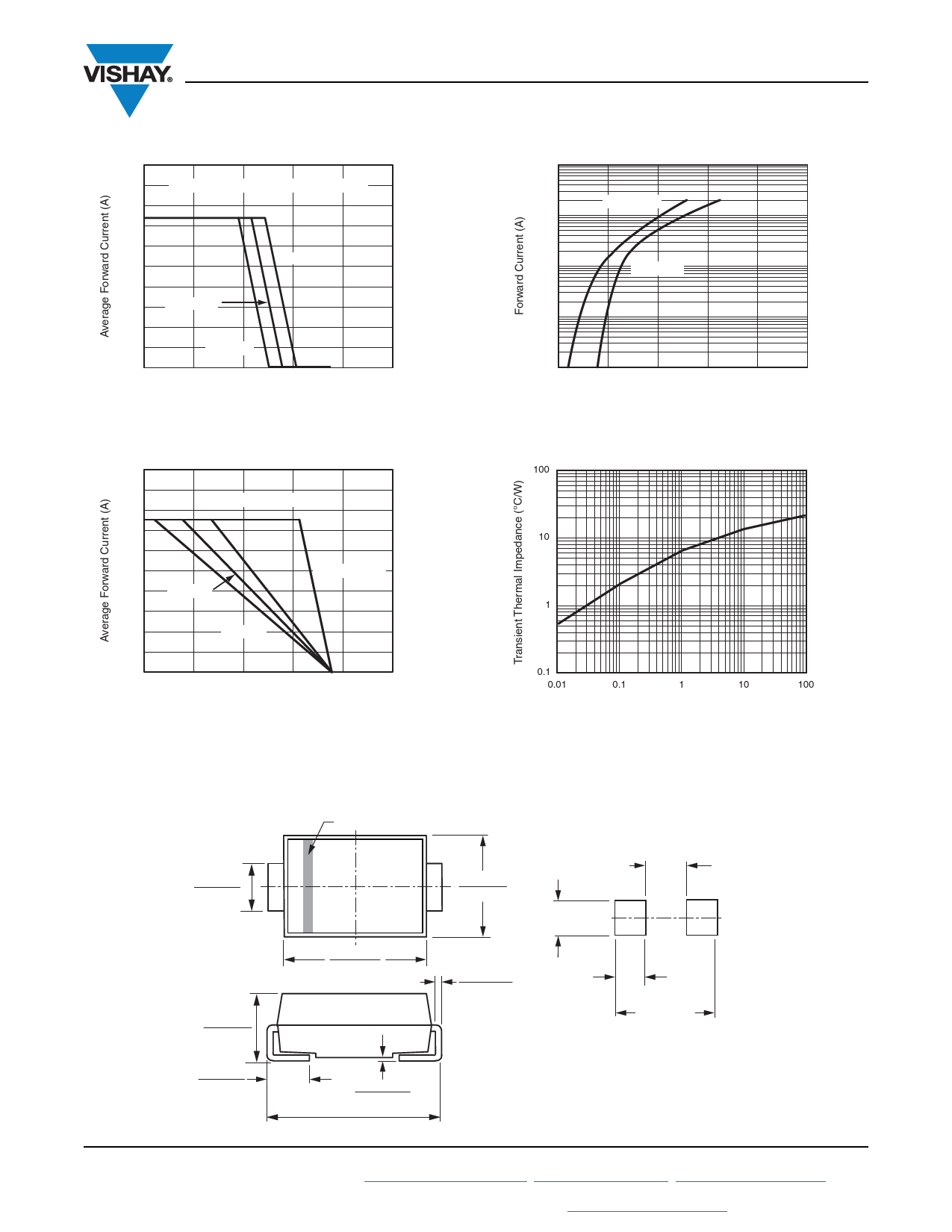
Figure 3. Max. Average Forward Current vs. Ambient Temperature
100
TJ = 150 °C
10
1
TJ = 25 °C
0.1
0.01
0
0.4
0.8
1.2
1.6
2.0
Forward Voltage (V)
Figure 5. Max. Forward Current vs. Forward Voltage
2.0
100
VR = 0 V, Half Sine-Wave
1.6
10
1.2
100 K/W
RthJA = 25 K/W
0.8 125 K/W
1
0.4
150 K/W
0
0
40
80
120
160
200
Ambient Temperature (°C)
Figure 4. Max. Average Forward Current vs. Ambient Temperature
0.1
0.01
0.1
1
10
100
t - Heating Time (s)
Figure 6. Diode Capacitance vs. Reverse Voltage
PACKAGE OUTLINE DIMENSIONS in inches (millimeters)
DO-214AC (SMA)
Cathode Band
Mounting Pad Layout
0.065 (1.65)
0.049 (1.25)
0.110 (2.79)
0.100 (2.54)
0.066 (1.68)
MIN.
0.074 (1.88)
MAX.
0.090 (2.29)
0.078 (1.98)
0.177 (4.50)
0.157 (3.99)
0.012 (0.305)
0.006 (0.152)
0.060 (1.52)
MIN.
0.208
(5.28) REF.
0.060 (1.52)
0.030 (0.76)
0.008 (0.203)
0 (0)
0.208 (5.28)
0.194 (4.93)
Document Number: 86013 For technical questions within your region, please contact one of the following:
Revision: 21-Jan-08
PDD-Americas@vishay.com, PDD-Asia@vishay.com, PDD-Europe@vishay.com
www.vishay.com
3
Share Link: 