CY7C1325G-133BGC(2004) データシートの表示(PDF) - Cypress Semiconductor
部品番号
コンポーネント説明
メーカー
CY7C1325G-133BGC Datasheet PDF : 16 Pages
| |||
PRELIMINARY
CY7C1325G
Single Write Accesses Initiated by ADSC
This write access is initiated when the following conditions are
satisfied at clock rise: (1) CE1, CE2, and CE3 are all asserted
active, (2) ADSC is asserted LOW, (3) ADSP is deasserted
HIGH, and (4) the write input signals (GW, BWE, and BW[A:B])
indicate a write access. ADSC is ignored if ADSP is active LOW.
The addresses presented are loaded into the address register
and the burst counter/control logic and delivered to the
memory core. The information presented to DQ[A:D] will be
written into the specified address location. Byte writes are
allowed. During byte writes, BWA controls DQA, BWB controls
DQB. All I/Os are tri-stated when a write is detected, even a
byte write. Since this is a common I/O device, the
asynchronous OE input signal must be deasserted and the
I/Os must be tri-stated prior to the presentation of data to DQs.
As a safety precaution, the data lines are tri-stated once a write
cycle is detected, regardless of the state of OE.
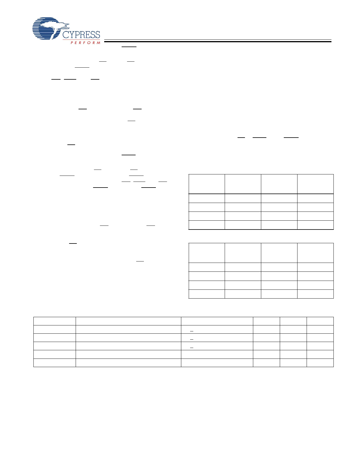
Burst Sequences
The CY7C1325G provides an on-chip two-bit wraparound
burst counter inside the SRAM. The burst counter is fed by
A[1:0], and can follow either a linear or interleaved burst order.
The burst order is determined by the state of the MODE input.
A LOW on MODE will select a linear burst sequence. A HIGH
on MODE will select an interleaved burst order. Leaving
MODE unconnected will cause the device to default to a inter-
leaved burst sequence.
Sleep Mode
The ZZ input pin is an asynchronous input. Asserting ZZ
places the SRAM in a power conservation “sleep” mode. Two
clock cycles are required to enter into or exit from this “sleep”
mode. While in this mode, data integrity is guaranteed.
Accesses pending when entering the “sleep” mode are not
considered valid nor is the completion of the operation
guaranteed. The device must be deselected prior to entering
the “sleep” mode. CEs, ADSP, and ADSC must remain
inactive for the duration of tZZREC after the ZZ input returns
LOW.
.
Interleaved Burst Address Table
(MODE = Floating or VDD)
First
Address
A1, A0
Second
Address
A1, A0
Third
Address
A1, A0
Fourth
Address
A1, A0
00
01
10
11
01
00
11
10
10
11
00
01
11
10
01
00
Linear Burst Address Table (MODE = GND)
First
Address
A1, A0
00
01
10
11
Second
Address
A1, A0
01
10
11
00
Third
Address
A1, A0
10
11
00
01
Fourth
Address
A1, A0
11
00
01
10
ZZ Mode Electrical Characteristics
Parameter
IDDZZ
tZZS
tZZREC
tZZI
tRZZI
Description
Snooze mode standby current
Device operation to ZZ
ZZ recovery time
ZZ Active to snooze current
ZZ Inactive to exit snooze current
Test Conditions
Min.
Max.
Unit
ZZ > VDD – 0.2V
40
mA
ZZ > VDD – 0.2V
2tCYC
ns
ZZ < 0.2V
2tCYC
ns
This parameter is sampled
2tCYC
ns
This parameter is sampled
0
ns
Truth Table [2, 3, 4, 5, 6]
Cycle Description
Deselected Cycle,
Power-down
Address
Used
None
CE1 CE2 CE3 ZZ
H X XL
ADSP ADSC ADV WRITE OE
X
L
X
X
X
CLK
DQ
L-H tri-state
Deselected Cycle,
Power-down
None
L L XL
L
X
X
X
X L-H tri-state
Deselected Cycle,
Power-down
None
L XHL
L
X
X
X
X L-H tri-state
Notes:
2. X = “Don't Care.” H = Logic HIGH, L = Logic LOW.
3. WRITE = L when any one or more Byte Write enable signals (BWA, BWB) and BWE = L or GW= L. WRITE = H when all Byte write enable signals (BWA, BWB),
BWE, GW = H.
4. The DQ pins are controlled by the current cycle and the OE signal. OE is asynchronous and is not sampled with the clock.
5. The SRAM always initiates a read cycle when ADSP is asserted, regardless of the state of GW, BWE, or BW[A: B]. Writes may occur only on subsequent clocks
after the ADSP or with the assertion of ADSC. As a result, OE must be driven HIGH prior to the start of the write cycle to allow the outputs to tri-state. OE is a
don't care for the remainder of the write cycle.
6. OE is asynchronous and is not sampled with the clock rise. It is masked internally during write cycles. During a read cycle all data bits are tri-state when OE is
inactive or when the device is deselected, and all data bits behave as output when OE is active (LOW).
Document #: 38-05518 Rev. *A
Page 5 of 16
Share Link: 