DS2720BU/TR データシートの表示(PDF) - Dallas Semiconductor -> Maxim Integrated
部品番号
コンポーネント説明
メーカー
DS2720BU/TR
Dallas Semiconductor -> Maxim Integrated
DS2720BU/TR Datasheet PDF : 21 Pages
| |||
DS2720
Table 1. DETAILED PIN DESCRIPTION
SYMBOL DESCRIPTION
Battery-Pack Positive Terminal Input. The device monitors the state of the battery
PLS
pack’s positive terminal through this pin in order to detect events such as the attachment
of a charger or the removal of a short circuit. Connect PLS to the pack positive terminal
through a 100W resistor.
Power-Switch Sense Input. The device wakes up from sleep mode when it senses the
PS
closure of a switch to VSS on this pin. PS has a high-impedance internal pullup.
DQ
Data Input/Out. 1-Wire data line. Open-drain output driver. Connect this pin to the
DATA terminal of the battery pack. DQ has an internal 0.5mA pull-down.
VSS
Device Ground. Connect directly to the negative terminal of the battery cell.
VDD
Power Supply Input. Connect VDD to the positive terminal of the battery cell through a
decoupling network.
Charge Pump Output. The internal charge pump regulates CP to 9V which supplies
CP
the ON state drive to the protection FETs. Connect a 0.1mF reservoir capacitor from CP
to VSS.
CC
Charge Protection Control Output. Controls an external N-channel high-side charge
protection FET.
DC
Discharge Protection Control Output. Controls an external N-channel high-side
discharge protection FET.
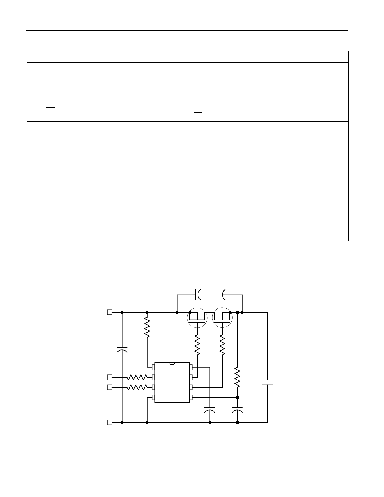
Figure 2. APPLICATION EXAMPLE
102
102
PACK+
PS
DATA
PACK-
100
102
1k
1k
DS2720
330
PLS CP
PS DC
DQ CC
330
VSS VDD
104
10
1-CELL Li+
104
4 of 21
Share Link: 